
7.8: Exercises
- Page ID
- 34248

Unless otherwise specified, use \(\beta = 100\).
7.8.1: Analysis Problems
1. Determine the input and output impedances of the circuit of Figure \(\PageIndex{1}\).
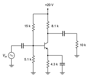
Figure \(\PageIndex{1}\)
2. Determine the load voltage for the circuit of Figure \(\PageIndex{1}\) if \(V_{in}\) is 10 mV.
3. Determine \(Z_{in}\), \(Z_{out}\), and the load voltage for the circuit of Figure \(\PageIndex{2}\) if \(V_{in}\) is 70 mV.
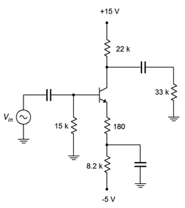
Figure \(\PageIndex{2}\)
4. Determine \(Z_{in}\), \(Z_{out}\), and the load voltage for the circuit of Figure \(\PageIndex{3}\) if \(V_{in}\) is 50 mV.
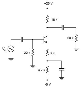
Figure \(\PageIndex{3}\)
5. Determine \(Z_{in}\), \(Z_{out}\), and the load voltage for the circuit of Figure \(\PageIndex{4}\) if \(V_{in}\) is 25 mV.
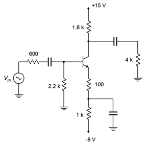
Figure \(\PageIndex{4}\)
6. Determine \(Z_{in}\), \(Z_{out}\), and the load voltage for the circuit of Figure \(\PageIndex{5}\) if \(V_{in}\) is 30 mV.
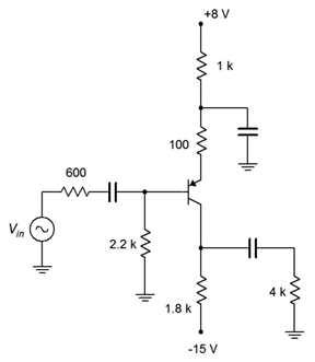
Figure \(\PageIndex{5}\)
7. Determine \(Z_{in}\), \(Z_{out}\), and the load voltage for the circuit of Figure \(\PageIndex{6}\) if \(V_{in}\) is 60 mV.
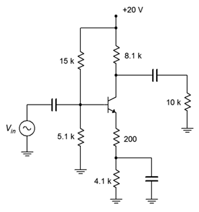
Figure \(\PageIndex{6}\)
8. Determine \(Z_{in}\), \(Z_{out}\), and the load voltage for the circuit of Figure \(\PageIndex{7}\) if \(V_{in}\) is 150 mV.
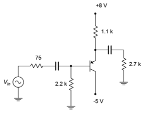
Figure \(\PageIndex{7}\)
9. Determine \(Z_{in}\), \(Z_{out}\), and the load voltage for the circuit of Figure \(\PageIndex{8}\) if \(V_{in}\) is 200 mV.
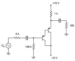
Figure \(\PageIndex{8}\)
10. Determine \(Z_{in}\), \(Z_{out}\), and the load voltage for the circuit of Figure \(\PageIndex{9}\) if \(V_{in}\) is 250 mV.
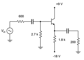
Figure \(\PageIndex{9}\)
11. Determine \(Z_{in}\), \(Z_{out}\), and the load voltage for the circuit of Figure \(\PageIndex{10}\) if \(V_{in}\) is 300 mV.
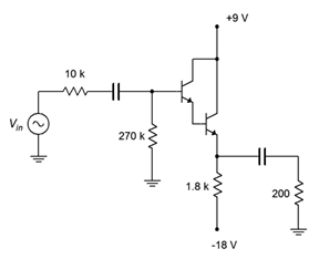
Figure \(\PageIndex{10}\)
12. Determine \(Z_{in}\), \(Z_{out}\), and the load voltage for the circuit of Figure \(\PageIndex{11}\) if \(V_{in}\) is 50 mV.
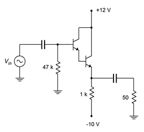
Figure \(\PageIndex{11}\)
13. Determine \(Z_{in}\), \(Z_{out}\), and the load voltage for the circuit of Figure \(\PageIndex{12}\) if \(V_{in}\) is 2 mV.
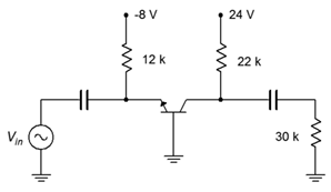
Figure \(\PageIndex{12}\)
7.8.2: Design Problems
14. Redesign the circuit of Figure \(\PageIndex{2}\) to halve the existing gain while keeping the Q point where it is currently.
15. By using a Darlington pair, redesign the circuit of Figure \(\PageIndex{3}\) to double \(Z_{in}\).
16. Redesign the circuit of Figure \(\PageIndex{3}\) so that it exhibits the same performance parameters but uses a PNP device.
17. Redesign the circuit of Figure \(\PageIndex{5}\) to double the existing gain while keeping the Q point where it is currently.
18. Redesign the circuit of Figure \(\PageIndex{7}\) so that it exhibits the same performance parameters but uses an NPN device.
7.8.3: Challenge Problems
19. Determine the gain and input impedance for the circuit of Figure \(\PageIndex{13}\). \(V_{CC}\) = 20 V, \(V_{EE}\) = −10 V, \(R_B\) = 18 k\(\Omega\), \(R_{E1}\)= 10 k\(\Omega\), \(R_{C1}\) = 12 k\(\Omega\), \(R_1\) = 33 k\(\Omega\), \(R_2\) = 15 k\(\Omega\), \(R_{E2}\) = 5.6 k\(\Omega\), \(R_{SW}\) = 400 k\(\Omega\), \(R_{C2}\) = 6.8 k\(\Omega\), \(R_L\) = 24 k\(\Omega\).
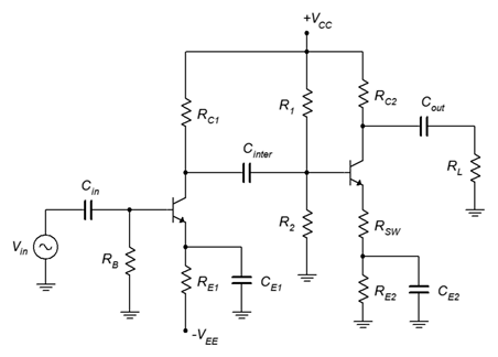
Figure \(\PageIndex{13}\)
20. For the circuit of Figure \(\PageIndex{10}\), replace its load resistor with the circuit of Figure \(\PageIndex{6}\) and determine the combined gain and input impedance of the system.
7.8.4: Computer Simulation Problems
21. Use a transient analysis to verify the load voltage of problem 3.
22. Use a transient analysis to verify the load voltage of problem 4.
23. Use a transient analysis to verify the load voltage of problem 8.
24. Consider the amplifier of Figure \(\PageIndex{1}\). Replace the 4.3 k\(\Omega\) emitter resistor with a potentiometer of the same value. Connect the wiper arm to the emitter bypass capacitor. Run several transient analyses at different pot settings (0%, 25%, 50%, etc.). What can you conclude from the results?