
9.2: The Class B Configuration
- Page ID
- 25439

\( \newcommand{\vecs}[1]{\overset { \scriptstyle \rightharpoonup} {\mathbf{#1}} } \)
\( \newcommand{\vecd}[1]{\overset{-\!-\!\rightharpoonup}{\vphantom{a}\smash {#1}}} \)
\( \newcommand{\dsum}{\displaystyle\sum\limits} \)
\( \newcommand{\dint}{\displaystyle\int\limits} \)
\( \newcommand{\dlim}{\displaystyle\lim\limits} \)
\( \newcommand{\id}{\mathrm{id}}\) \( \newcommand{\Span}{\mathrm{span}}\)
( \newcommand{\kernel}{\mathrm{null}\,}\) \( \newcommand{\range}{\mathrm{range}\,}\)
\( \newcommand{\RealPart}{\mathrm{Re}}\) \( \newcommand{\ImaginaryPart}{\mathrm{Im}}\)
\( \newcommand{\Argument}{\mathrm{Arg}}\) \( \newcommand{\norm}[1]{\| #1 \|}\)
\( \newcommand{\inner}[2]{\langle #1, #2 \rangle}\)
\( \newcommand{\Span}{\mathrm{span}}\)
\( \newcommand{\id}{\mathrm{id}}\)
\( \newcommand{\Span}{\mathrm{span}}\)
\( \newcommand{\kernel}{\mathrm{null}\,}\)
\( \newcommand{\range}{\mathrm{range}\,}\)
\( \newcommand{\RealPart}{\mathrm{Re}}\)
\( \newcommand{\ImaginaryPart}{\mathrm{Im}}\)
\( \newcommand{\Argument}{\mathrm{Arg}}\)
\( \newcommand{\norm}[1]{\| #1 \|}\)
\( \newcommand{\inner}[2]{\langle #1, #2 \rangle}\)
\( \newcommand{\Span}{\mathrm{span}}\) \( \newcommand{\AA}{\unicode[.8,0]{x212B}}\)
\( \newcommand{\vectorA}[1]{\vec{#1}} % arrow\)
\( \newcommand{\vectorAt}[1]{\vec{\text{#1}}} % arrow\)
\( \newcommand{\vectorB}[1]{\overset { \scriptstyle \rightharpoonup} {\mathbf{#1}} } \)
\( \newcommand{\vectorC}[1]{\textbf{#1}} \)
\( \newcommand{\vectorD}[1]{\overrightarrow{#1}} \)
\( \newcommand{\vectorDt}[1]{\overrightarrow{\text{#1}}} \)
\( \newcommand{\vectE}[1]{\overset{-\!-\!\rightharpoonup}{\vphantom{a}\smash{\mathbf {#1}}}} \)
\( \newcommand{\vecs}[1]{\overset { \scriptstyle \rightharpoonup} {\mathbf{#1}} } \)
\(\newcommand{\longvect}{\overrightarrow}\)
\( \newcommand{\vecd}[1]{\overset{-\!-\!\rightharpoonup}{\vphantom{a}\smash {#1}}} \)
\(\newcommand{\avec}{\mathbf a}\) \(\newcommand{\bvec}{\mathbf b}\) \(\newcommand{\cvec}{\mathbf c}\) \(\newcommand{\dvec}{\mathbf d}\) \(\newcommand{\dtil}{\widetilde{\mathbf d}}\) \(\newcommand{\evec}{\mathbf e}\) \(\newcommand{\fvec}{\mathbf f}\) \(\newcommand{\nvec}{\mathbf n}\) \(\newcommand{\pvec}{\mathbf p}\) \(\newcommand{\qvec}{\mathbf q}\) \(\newcommand{\svec}{\mathbf s}\) \(\newcommand{\tvec}{\mathbf t}\) \(\newcommand{\uvec}{\mathbf u}\) \(\newcommand{\vvec}{\mathbf v}\) \(\newcommand{\wvec}{\mathbf w}\) \(\newcommand{\xvec}{\mathbf x}\) \(\newcommand{\yvec}{\mathbf y}\) \(\newcommand{\zvec}{\mathbf z}\) \(\newcommand{\rvec}{\mathbf r}\) \(\newcommand{\mvec}{\mathbf m}\) \(\newcommand{\zerovec}{\mathbf 0}\) \(\newcommand{\onevec}{\mathbf 1}\) \(\newcommand{\real}{\mathbb R}\) \(\newcommand{\twovec}[2]{\left[\begin{array}{r}#1 \\ #2 \end{array}\right]}\) \(\newcommand{\ctwovec}[2]{\left[\begin{array}{c}#1 \\ #2 \end{array}\right]}\) \(\newcommand{\threevec}[3]{\left[\begin{array}{r}#1 \\ #2 \\ #3 \end{array}\right]}\) \(\newcommand{\cthreevec}[3]{\left[\begin{array}{c}#1 \\ #2 \\ #3 \end{array}\right]}\) \(\newcommand{\fourvec}[4]{\left[\begin{array}{r}#1 \\ #2 \\ #3 \\ #4 \end{array}\right]}\) \(\newcommand{\cfourvec}[4]{\left[\begin{array}{c}#1 \\ #2 \\ #3 \\ #4 \end{array}\right]}\) \(\newcommand{\fivevec}[5]{\left[\begin{array}{r}#1 \\ #2 \\ #3 \\ #4 \\ #5 \\ \end{array}\right]}\) \(\newcommand{\cfivevec}[5]{\left[\begin{array}{c}#1 \\ #2 \\ #3 \\ #4 \\ #5 \\ \end{array}\right]}\) \(\newcommand{\mattwo}[4]{\left[\begin{array}{rr}#1 \amp #2 \\ #3 \amp #4 \\ \end{array}\right]}\) \(\newcommand{\laspan}[1]{\text{Span}\{#1\}}\) \(\newcommand{\bcal}{\cal B}\) \(\newcommand{\ccal}{\cal C}\) \(\newcommand{\scal}{\cal S}\) \(\newcommand{\wcal}{\cal W}\) \(\newcommand{\ecal}{\cal E}\) \(\newcommand{\coords}[2]{\left\{#1\right\}_{#2}}\) \(\newcommand{\gray}[1]{\color{gray}{#1}}\) \(\newcommand{\lgray}[1]{\color{lightgray}{#1}}\) \(\newcommand{\rank}{\operatorname{rank}}\) \(\newcommand{\row}{\text{Row}}\) \(\newcommand{\col}{\text{Col}}\) \(\renewcommand{\row}{\text{Row}}\) \(\newcommand{\nul}{\text{Nul}}\) \(\newcommand{\var}{\text{Var}}\) \(\newcommand{\corr}{\text{corr}}\) \(\newcommand{\len}[1]{\left|#1\right|}\) \(\newcommand{\bbar}{\overline{\bvec}}\) \(\newcommand{\bhat}{\widehat{\bvec}}\) \(\newcommand{\bperp}{\bvec^\perp}\) \(\newcommand{\xhat}{\widehat{\xvec}}\) \(\newcommand{\vhat}{\widehat{\vvec}}\) \(\newcommand{\uhat}{\widehat{\uvec}}\) \(\newcommand{\what}{\widehat{\wvec}}\) \(\newcommand{\Sighat}{\widehat{\Sigma}}\) \(\newcommand{\lt}{<}\) \(\newcommand{\gt}{>}\) \(\newcommand{\amp}{&}\) \(\definecolor{fillinmathshade}{gray}{0.9}\)Class B operation is defined as having AC collector current flow 180\(^{\circ}\) out of the cycle. Consequently, in order to amplify the entire signal, two devices will be needed. Further, we will need to pay attention to how the two waveform halves are “stitched together” as this could be a problem area. The obvious question at this point is, why do we bother separating the positive and negative half-waves if it leads to circuit complexity and possible waveform issues? The answer is improved efficiency.
In the previous chapter we discovered that class A amplifiers are not efficient. In fact, at best they only transform 25% of the DC input power into useful load power. Why does this occur and how does the class B topology address this situation?
The basic idea of class B is to push the Q point down so that it is sitting right at cutoff on the AC load line. This means that \(I_{CQ}\) is 0 A and virtually no power is drawn from the supply at idle. Locating the Q point at cutoff also means that the transistor will immediately clip the negative portion of the wave. Consequently, we will need a mirror image circuit to produce that portion (and which will clip the positive portion).
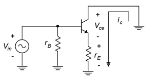
Figure \(\PageIndex{1}\): Voltage follower simplified AC circuit.
To gain a better understanding of how class B operation works, consider the simplified AC circuit of a voltage follower shown in Figure \(\PageIndex{1}\). If we situate the Q point directly at \(v_{CE(cutoff)}\) then the associated \(I_{CQ}\) is 0 A. As the input signal swings positive, the collector current increases. As it does so, the voltage across the load \((r_E)\) begins to increase and the voltage across the transistor's collector-emitter begins to decrease (due to KVL). When the input signal swings negative, the transistor is turned off. As a result, no collector current is created, no voltage is developed across the load and \(v_{CE}\) stays at cutoff. It is as if the input waveform has been half-wave rectified. This action is shown in Figure \(\PageIndex{2}\). As the input signal swings positive, the operating point slides up the load line, moving toward saturation, and this increased current creates a load voltage that follows the input signal. In contrast, when the input tries to swing negative, there is no place else to go on the load line and the negative portion of the wave is simply clipped.
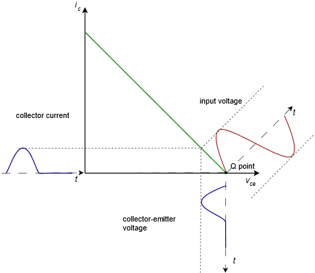
Figure \(\PageIndex{2}\): AC load line for class B operation.
If we made a PNP version of the circuit depicted in Figure \(\PageIndex{1}\), the exact opposite would happen: the amplifier would reproduce the negative portion of the wave and clip the positive portion. The next question is, how do we bias the transistor at cutoff and splice together the NPN and PNP versions into a workable whole?
Let's begin by making two bare-bones emitter followers, one NPN and the other PNP. We'll connect their emitters together and tie that to the load. We'll connect the NPN's collector directly to a DC supply and the PNP's collector to ground. Remember, collector resistors will not be needed because these are followers. We will include no biasing components on the base because we want to set \(I_{CQ}\) to 0 A. We will also have to add input and output capacitors to prevent the source and load from inadvertently shorting out or shunting portions of the DC circuit. The result is seen in Figure \(\PageIndex{3}\).
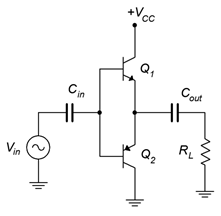
Figure \(\PageIndex{3}\): Prototype Class B circuit.
With no signal supplied, both transistors must be off. This is because their bases are tied together, and without some other applied potential, both base-emitter voltages must be zero. Assuming \(Q_1\) and \(Q_2\) are matched, the power supply voltage should split evenly between them, leaving half of \(V_{CC}\) at the emitters. This potential also appears across \(C_{out}\), preventing the DC voltage from reaching \(R_L\).
When the input signal goes positive, it raises \(V_{B1}\) and \(V_{B2}\) above 0.5 \(V_{CC}\). This keeps \(Q_2\) off but turns on \(Q_1\). Current is now free to flow down through \(Q_1\) and into the load. When the input signal swings negative, the inverse happens: \(Q_1\) is turned off and \(Q_2\) is turned on. This allows current to flow up from the load and down through \(Q_2\) (if this is confusing, remember that a DC voltage had already been established across \(C_{out}\) that is equal to 0.5 \(V_{CC}\) and this is what allows the current to flow from ground up through \(R_L\) and then down through \(Q_2\) as \(Q_2\) begins to conduct). You can think of \(Q_1\) pushing current into the load (sourcing) and \(Q_2\) pulling current from the load (sinking). Consequently, class B amplifiers are sometimes called a push-pull amplifiers.
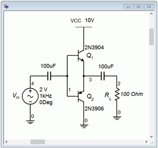
Figure \(\PageIndex{4}\): Prototype Class B circuit in simulator.
To see how well this prototype works, we'll enter a version into a simulator, as shown in Figure \(\PageIndex{4}\). A transient analysis is performed with the results shown in Figure \(\PageIndex{5}\).
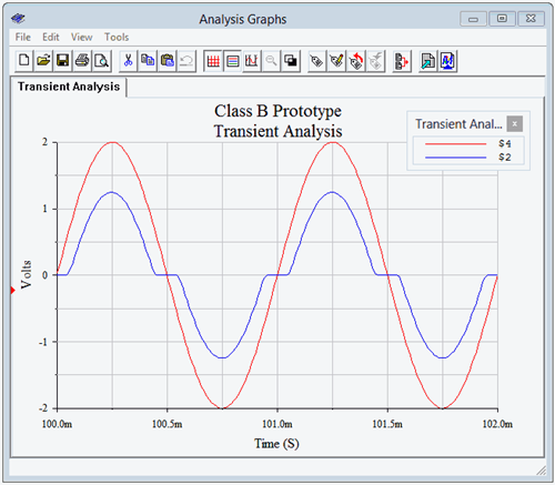
Figure \(\PageIndex{5}\): Transient analysis of prototype Class B circuit.
Clearly, there are issues with the output waveform (node 2, in blue). First off, the signal amplitude is noticeably smaller than the 2 volt peak input signal. The second issue is the bizarre “flat spotting” of the output waveform near the zero-crossing points. It turns out that these two problems are manifestations of the same root cause. If we look carefully at the peaks, we can get a clue as to what is going on. The peak output voltage is about 0.75 volts below the input, or just about one PN junction forward potential. The problem is that the input signal will not truly turn on the NPN transistor until the signal exceeds approximately 0.7 volts or drops below −0.7 volts for the PNP side. That region between −0.7 volts and +0.7 volts is a dead zone that the amplifier will not respond to. Essentially, the amplifier “rips out” anything between \(\pm\)0.7 volts. This is a gross form of distortion and goes by many names including notch distortion and cross-over distortion. The particularly nasty part about this form of distortion is that it hits small signals worse than large signals. Most other forms of nonlinearities tend to get worse as the signal level increases.
9.2.1: Class AB Operation
The basic solution to this problem is to provide a small idle current so that the transistors are almost on. In this way, only a very small input signal will be needed to turn on the devices. As this would slightly increase the conduction angle, this form of operation is referred to as class AB operation. One potential solution is to add a voltage divider as depicted in Figure \(\PageIndex{6}\).
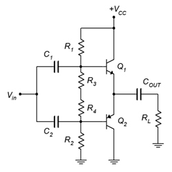
Figure \(\PageIndex{6}\): Prototype Class AB circuit.
This circuit uses a symmetrical layout: everything above a horizontal line drawn through the middle is echoed by a component below the line. In other words, \(R_1 = R_2\), \(R_3 = R_4\), \(C_1 = C_2\), and \(Q_1\) and \(Q_2\) are a complimentary pair. The divider is configured so that the voltage drops across \(R_3\) and \(R_4\) are about 0.7 volts each.
Properly designed, the circuit of Figure \(\PageIndex{6}\) will reduce notch distortion. Unfortunately, it has other problems. The first issue involves the three capacitors. \(C_{OUT}\) in particular might be quite large. These can be removed if we went to a symmetrical bipolar power supply. Instead of running the PNP's collector to ground, we'll tie it to a negative DC supply. To keep the same total voltage, we'll set \(Q_1\)'s collector to half of the original \(V_{CC}\) and \(Q_2\)'s collector to half of the original \(V_{CC}\) but negative. On the input side, we could run the input signal to the junction of \(R_3\) and \(R_4\).
The second issue plaguing the circuit of Figure \(\PageIndex{6}\) is the stability of the bias. The voltage divider resistors have to be very accurate in order to set the transistors right where we want them and stability is a concern. The problem is that we are trying to use a device with a linear current-voltage characteristic (a resistor) to match the exponential current-voltage characteristic of a PN junction. This problem is exacerbated by the fact that these devices will drift with temperature, and drift in different ways. The solution to this problem is to use a device with better matching characteristics. What better device to match a PN junction than another PN junction?
9.2.2: The Current Mirror
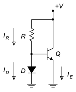
Figure \(\PageIndex{7}\): A simple current mirror.
Consider the circuit shown in Figure \(\PageIndex{7}\). This is called a current mirror. Here is how it works: First, look at the divider between \(R\) and \(D\). The voltage across \(R\) must equal the supply voltage minus the diode drop, or approximately \(V − 0.7\). This sets up a current, \(I_R\). If the base current is small enough to ignore, this same current flows down through the diode as \(I_D\). This diode current sets up a specific voltage across the diode (somewhere in the vicinity of 0.7 volts although the exact voltage is not important). Because the diode is in parallel with the base-emitter junction, then \(V_{BE} = V_D\). If the transconductance curve (I-V curve) of the transistor is identical to that of the diode, then the emitter current must be the same as the diode current. Any change in the diode current would cause a slight change in diode voltage, and since diode voltage and base-emitter voltage are the same, then the emitter current must change in response. In other words, the emitter current mirrors the diode current. We can program the diode current (and hence, the emitter current) by setting an appropriate value for \(R\). Whatever the current through \(R\) is, that's also the collector current.
The idea of the current mirror is used with great effect in integrated circuits where it is easy to match device characteristics. When it comes to discrete components, it is not nearly so easy to match a diode to a transistor. Fortunately, we don't have to have a perfect match. Simply using any signal diode will provide a much better match for \(V_{BE}\) than using a resistor. Although the diode current won't match the collector current precisely, the bias will be more stable and the components will track much better than when using a resistor.
Combining these ideas leads us to the circuit of Figure \(\PageIndex{8}\). This is our first practical class B amplifier with the potential for decent values of distortion and stability.
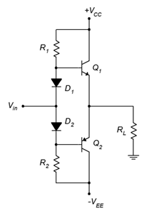
Figure \(\PageIndex{8}\): Class B amplifier with diode bias and bipolar supplies.
One thing that sometimes bothers people when they first see a diode biased amplifier is how the AC signal will pass through the diodes to the bases. At first glance, it appears that the positive portion of the input signal would be “going the wrong way” against diode \(D_1\). What we need to remember is that \(D_1\) is already forward-biased due to the DC supply and surrounding resistors. The signal won't see an open, it will see the dynamic resistance of the diode.2
9.2.3: Class B Circuit Maximums
Now that we have a workable circuit, we need to derive formulas for the endpoints of the AC load line, meaning \(v_{CE(cutoff)}\) and \(i_{C(sat)}\), and determine the compliance. The first item of note is cutoff. Because the two transistors will split the available supply, \(V_{CEQ}\) will always equal half of the total supply. Further, we have biased these devices at cutoff, and therefore
\[v_{CE(cutoff)} = V_{CEQ} = 0.5 \cdot \text{ Total DC Supply} \label{9.1} \]
In the case of a bipolar supply, that's the same as one of the two sides. Because the class B uses two transistors, peak compliance will be the same as cutoff.
\[Compliance_{peak} = V_{CEQ} = 0.5 \cdot \text{ Total DC Supply} \label{9.2} \]
The maximum voltage rating of the transistors will occur when they are off. In that instance, if the opposite transistor is fully conducting it will have a negligible voltage across its collector-emitter. Consequently, the off-state transistor can see the entire power supply.
\[BV_{CEO} = \text{ Total DC Supply} \label{9.3} \]
The saturation current is dictated by the compliance and the load. The only thing that limits AC current is the load. Therefore
\[i_{C(sat )} = \frac{Compliance_{peak}}{r_L} \label{9.4} \]
Based on that, we can say
\[P_{load (max)} = \frac{{Compliance_{RMS}}^2}{r_L} \label{9.5} \]
Before we go any further, there is an important item to note about the circuit of Figure \(\PageIndex{8}\) (and the variants we shall discuss). If you take another look at the circuit you will see that there is nothing in the collector-emitter line to limit DC current. In fact, if we were to plot the DC load alongside the AC load, we'd get something like Figure \(\PageIndex{9}\).
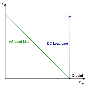
Figure \(\PageIndex{9}\): Comparison of AC and DC load lines for class B operation
The DC load line goes straight up. There is no saturation current value short of infinity. What this really means is that if we're not careful with the bias, it is possible to destroy the transistors. The same is true if we accidentally short the load. A quick examination of Equations \ref{9.4} and \ref{9.5} shows that a shorted load condition would lead to huge currents and powers, and destroy the transistors in the process. With an audio amplifier, this could happen if one of the strands of loudspeaker wire unraveled and touched the adjacent lead. Obviously, not a happy situation unless you prefer the smell of burnt silicon over the sound of music. We will examine means of protecting the transistors from accidental overloads later in the chapter.
9.2.4: Class B Power Dissipation
Transistor power dissipation for the class B configuration is a bit trickier than it was for the class A. The idle (Q point) power dissipation is very low. It is found by multiplying \(I_{CQ}\) by \(V_{CEQ}\). \(I_{CQ}\) is generally set at a few percent of \(i_{C(sat)}\) so it's obviously way below the maximum load power. Unlike the class A design, \(P_{DQ}\) does not represent the worst case for class B.
To determine the worst case transistor power dissipation, we begin by describing the current and voltage waveforms during the conduction phase of the NPN. The collector current will appear as the positive half of a sine wave. The maximum case has the current starting at zero and peaking at \(i_{C(sat)}\) (or alternately, \(V_{CEQ}/r_L\)). For \(v_{CE}\), it starts at \(V_{CEQ}\) and then swings down to zero as a negative half sine.
Nothing says that the maximum load power case must cause the maximum transistor dissipation. In fact, we saw this wasn't the case for class A. Consequently, we will introduce a coefficient, \(k\), that represents the percentage of the maximum current. We now arrive at our general equations for transistor current and voltage for the first half cycle.
\[i_C = k \frac{V_{CEQ}}{r_L} \sin 2 \pi ft \label{9.6} \]
\[v_{CE} = V_{CEQ} (1−k \sin 2 \pi ft) \label{9.7} \]
Where \(0 \leq k \leq 1\)
For convenience, we'll set \(2 \pi f\) to 1. To get the power dissipation, we find the product of the transistor's current and voltage.
\[P_D = i_C v_{CE} \nonumber \]
\[P_D = k \frac{V_{CEQ}}{r_L} \sin t \times V_{CEQ} (1−k \sin t) \nonumber \]
\[P_D = \frac{{V_{CEQ}}^2}{r_L} k \sin t− \frac{{V_{CEQ}}^2}{r_L} k^2 \sin^2 t \nonumber \]
\[P_D = \frac{{V_{CEQ}}^2}{r_L} (k \sin t −k^2 \sin^2 t) \nonumber \]
Remove ugly \(\sin^2\) term...
\[P_D = \frac{{V_{CEQ}}^2}{r_L} \left( k \sin t + \frac{k^2}{2} \cos 2t − \frac{k^2}{2} \right) \nonumber \]
..and integrate to get:
\[P_D = \frac{{V_{CEQ}}^2}{r_L} \left(−k \cos t − \frac{k^2}{4} \sin 2t − \frac{k^2 t}{2} \right) |_0^\pi \nonumber \]
Note that \(\frac{V_{CEQ}^2}{r_L} = 2 P_{load (max)}\) This is a constant, so replace it to simplify and then evaluate the expression. Finally, divide by \(2 \pi\) to find the average over one full cycle.
\[P_D = \frac{2 P_{load (max)} \left( 2k − \frac{k^2 \pi}{2} − \frac{k^2 t}{2} \right)}{2 \pi} \\ P_D = 2 P_{load (max)} \left( \frac{k}{\pi} − \frac{k^2}{4} \right) \label{9.8} \]
Equation \ref{9.8} is the general case. For the worst case, we need the min/max \(k\) value. We will take the derivative of Equation \ref{9.8} and then set it to zero to find the worst case value of \(k\).
\[P_D = 2 P_{load (max )} \left( \frac{k}{\pi} − \frac{k^2}{4} \right) \nonumber \]
\[\frac{d P_D}{d k} = 2 P_{load (max)} \left( \frac{1}{\pi} − \frac{k}{2} \right) \nonumber \]
Worst case occurs at \(k = 2/ \pi \). This means that only \(2/ \pi \), or 63.7%, of the load line is used at maximal heating of the transistor. 63.7% of the load line corresponds to a load power of about 40% of \(P_{load(max)}\) (i.e., \(0.637^2\)). We now substitute this value back into Equation \ref{9.8} to find the worst case \(P_D\).
\[P_D = 2 P_{load (max)} \left( \frac{2/ \pi}{\pi} − \frac{(2/ \pi )^2}{4} \right) \\ P_D = \frac{2}{\pi^2} P_{load (max )} \approx \frac{ P_{load (max)}}{5} \label{9.9} \]
The end result is that when the load is receiving about 40% of its maximum power, the transistors will be at their hottest and will be dissipating approximately 20% of the maximum load power (or about half of the power delivered to the load at that point). Thus, if a class B amplifier is rated to produce a maximum load power of 100 watts, the transistors will get their hottest when the load is receiving 40 watts, and each transistor will be dissipating 20 watts. The transistors will be dissipating less power when the load is at maximum. This is easily verified by substituting \(k = 1\) into Equation \ref{9.8}. The result is a power dissipation of 13.7% of maximum load power, or 13.7 watts for the preceding example.
To help gain a deeper understanding of precisely what's happening here, the transistor waveforms are plotted in Figures \(\PageIndex{10}\) and \(\PageIndex{11}\). The maximum load power case is presented in Figure \(\PageIndex{10}\). Here, we see the full \(i_C\) and \(v_{CE}\) swings. Note that when \(i_C\) is maximum, \(v_{CE}\) is 0, hence the power is 0. In contrast, Figure \(\PageIndex{11}\) shows the worst case. Collector current peaks at just under 64% of maximum but \(v_{CE}\) drops to only about 36% rather than 0% of its maximum. This results in a power dissipation curve with considerably greater area underneath it, indicating a higher average power.
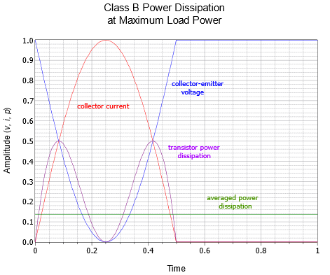
Figure \(\PageIndex{10}\): Class B transistor power dissipation at \(P_{Load(max)}\).
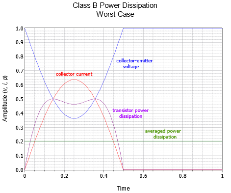
Figure \(\PageIndex{11}\): Class B transistor power dissipation, worst case.
Finally, it is worth remembering that the reactive load issues discussed for class A amplifiers still apply to class B amplifiers. Loads with a complex impedance may be harder to drive than the ideal purely resistive loads examined here. Therefore, we may have to over-rate the transistors above \(P_{load(max)} /5\). As a side note, the AC load line for a class B amplifier with a reactive load will appear as an ellipse that has been cut in half (refer back to Figure 8.4.5 and imagine a horizontal cut line running through the Q point).
9.2.5: Class B Efficiency
Efficiency is defined as useful output or load power versus supplied DC power.
\[\eta = \frac{P_{out}}{P_{i n}} = \frac{P_{load (max )}}{P_{DC}} \nonumber \]
This is dynamic for class B amplifiers. At \(P_{load(max)}\) the DC supply is delivering the full voltage of \(2 V_{CEQ}\) and the corresponding peak value of the current is \(i_{C(sat)}\).
\[i_{C(sat )} = \frac{V_{CEQ}}{r_L} \nonumber \]
The average of this over a half-cycle is
\[i_{C(avg )} = \frac{1}{\pi} \times \frac{V_{CEQ}}{r_L} \nonumber \]
Therefore, the supplied power must be
\[P_{DC} = 2V_{CEQ} i_{C(sat)} \nonumber \]
\[P_{DC} = 2V_{CEQ} \times \frac{1}{\pi} \frac{V_{CEQ}}{r_L} \nonumber \]
\[P_{DC} = \frac{2}{\pi} \times \frac{{V_{CEQ}}^2}{r_L} \nonumber \]
As noted previously V CEQ 2 r L = 2 Pload (max) therefore
\[P_{DC} = \frac{4}{\pi} \times P_{load (max)} \nonumber \]
Finally, substitute this expression back into the original definition for efficiency.
\[\eta_{max} = \frac{P_{load (max)}{{P_{DC}} \nonumber \]
\[\eta_{max} = \frac{P_{load (max)}}{\frac{4}{\pi} P_{load (max)}} \nonumber \]
\[\eta_{max} = \frac{\pi}{4} \nonumber \]
\[\eta_{max} \approx 78.5\% \nonumber \]
We find that the maximum theoretical efficiency of a class B amplifier is over three times that of a class A amplifier.
Time for an example.
Example \(\PageIndex{1}\)
The amplifier shown in Figure \(\PageIndex{12}\) is driving a nominal 8 \( \Omega \) loudspeaker. Determine the compliance, maximum load power and worst case transistor dissipation. Also estimate \(Z_{in}\) assuming \(\beta = 50\) and determine the transistor ratings for maximum current and \(BV_{CEO}\).
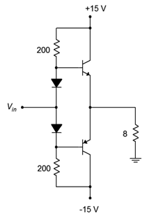
Figure \(\PageIndex{12}\): Schematic for Example \(\PageIndex{1}\).
By inspection, \(V_{CEQ} = 15\) V. This is the peak compliance.
\[compliance = 15 V peak = 10.6 V RMS \nonumber \]
Given the compliance, we can use power law to find the load power
\[P_{load (max)} = \frac{{Compliance_{RMS}}^2}{R_L} \nonumber \]
\[P_{load (max)} = \frac{(0.707 \times 15V)^2}{8 \Omega } \nonumber \]
\[P_{load (max)} = 14W \nonumber \]
That's not huge but it might be enough to irritate the neighbors.
The transistors' worst case power dissipation is
\[P_D = \frac{P_{load (max)}}{5} \nonumber \]
\[P_D = \frac{14W}{5} \nonumber \]
\[P_D = 2.8 W \nonumber \]
The breakdown voltage is the entire supply so \(BV_{CEO} > 30\) V. The maximum current through the transistors is the same as the maximum load current or \(i_{C(sat)}\).
\[i_{C(sat )} = \frac{V_{CEQ}}{r_L} \nonumber \]
\[i_{C(sat )} = \frac{15 V}{8 \Omega} \nonumber \]
\[i_{C(sat )} = 1.88 A \nonumber \]
The input impedance is found in the usual manner but with a minor twist. \(Z_{in(base)}\) is approximately equal to \(\beta r_L\), or about 400 \( \Omega \). Only one transistor is on at any given time, though, so this is in parallel with the two 200 \( \Omega \) biasing resistors but not the other \(Z_{in(base)}\) (the “off” transistor has a very high input impedance because it is not conducting). This leaves a \(Z_{in(base)}\) of about 80 \( \Omega \), or ten times the load impedance.
Computer Simulation
To verify the basic operation of a class B amplifier, the circuit of Figure \(\PageIndex{13}\) is entered into a simulator. The amplifier should clip just below the \(\pm\)10 volt power rails so a 10 volt peak source is used to verify this. Also, \(A_v\) should be about 1.
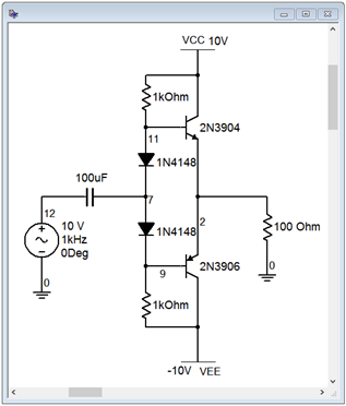
Figure \(\PageIndex{13}\): Class B amplifier in simulator.
The results of a transient analysis are shown in Figure \(\PageIndex{14}\). First, it is apparent that the voltage gain is approximately unity as the input and output waves are nearly coincident (with the exception of the clipped portion). Clipping occurs at about 8.5 volts. This is largely due to limiting from the biasing diodes. Once the input gets close in value to the power supply, the diodes become reverse-biased and the signal does not make it to the base. Thus, the output clips prematurely.
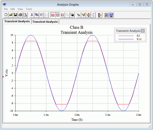
Figure \(\PageIndex{14}\): Class B amplifier transient analysis.
To verify earlier commentary regarding the biasing diodes, the circuit is modified so that the diodes are shorted out and the transient analysis is run again. The results are shown in Figure \(\PageIndex{15}\).
Two things should be apparent in the new simulation. First, the output waveform is suffering from obvious notch distortion. Therefore, we can be pleased that the biasing diodes have done their job to reduce this effect. The second item involves the compliance. The new output is not clipped. Granted, the lack of biasing diodes has reduced the signal by about 0.7 volts, but a careful examination of the output waveform shows that it has reached over 9 volts peak without clipping. In fact, if we increase the input to 12 volts peak, as in Figure \(\PageIndex{16}\), we can see that clipping occurs just under the power rails. Thus, the premature clipping is due to the diodes and their interaction with the power supplies and surrounding resistors. In short, we lose a little bit of compliance due to the diodes but that's much better than getting notch distortion.
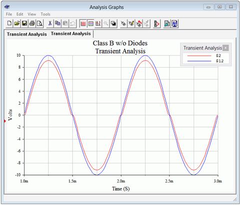
Figure \(\PageIndex{15}\): Class B amplifier transient analysis, without biasing diodes.
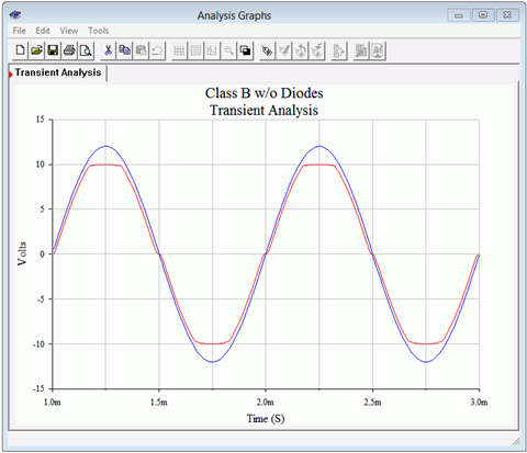
Figure \(\PageIndex{16}\): Class B amplifier transient analysis, without biasing diodes and showing clipping.
9.2.6: Direct Coupled Driver
The circuits we have examined offer both current gain and power gain but not voltage gain. In order to increase the signal voltage, some preceding voltage gain stages will most likely be needed. These stages can be connected to the previous class B follower circuits with coupling capacitors but this is not the most effective method. A more common technique is the use of a direct coupled driver.
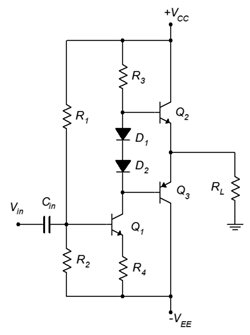
Figure \(\PageIndex{17}\): Class B amplifier with direct coupled driver.
A class B follower with a direct coupled driver stage is shown in Figure \(\PageIndex{17}\). What we've done here is combined an ordinary class A common emitter amplifier (in this case, using voltage divider bias) with a class B follower. The follower is positioned where the common emitter stage's collector resistor would be normally. This eliminates three components: the collector resistor, the interstage coupling capacitor, and the lower base biasing resistor of the class B output stage. The removal of the resistors raises the effective load resistance for the first stage, thus producing a higher voltage gain from the driver stage.
Biasing the direct coupled driver is not difficult if we remember one thing: the DC voltage across \(R_3\) must be equal to approximately \(V_{CC} − 0.7\) V. If this is not the case, the class B stage will not be symmetrical, or in other words, \(V_{CEQ2} \neq V_{CEQ3}\), and the final output will not be sitting at 0 VDC as it needs to. Knowing the value of \(R_3\) and its voltage, we can determine its current. This current flows down into \(Q_1\) as \(I_{CQ1}\). Knowing \(I_{CQ1}\), we can determine the voltage across \(R_4\) and eventually determine the appropriate divider ratio for \(R_1\) and \(R_2\) to achieve this value.
Example \(\PageIndex{2}\)
Using the two-stage amplifier of Figure \(\PageIndex{17}\), first determine values for \(R_1\) and \(R_2\) to obtain proper system bias. Determine the output compliance, maximum load power and worst case transistor dissipation. Also estimate \(A_v\). Assume \(\beta = 50\) for the output devices and 100 for the first stage. \(V_{CC} = 20\) V, \(V_{EE} = −20\) V, \(R_L = 16\) \( \Omega \), \(R_3 = 560\) \( \Omega \), \(R_4 = 75\) \( \Omega \).
For the output section (assuming it will be biased properly), by inspection, \(V_{CEQ} = 20\) V. This is the peak compliance.
\[compliance = 20 V peak = 14.1 V RMS \nonumber \]
Given the compliance, we can use power law to find the load power
\[P_{load (max)} = \frac{{Compliance_{RMS}}^2}{R_L} \nonumber \]
\[P_{load (max)} = \frac{(14.1 V)^2}{16 \Omega} \nonumber \]
\[P_{load (max)} = 12.5 W \nonumber \]
The transistors' worst case power dissipation is
\[P_D = \frac{P_{load (max)}{5} \nonumber \]
\[P_D = \frac{12.5W}{5} \nonumber \]
\[P_D = 2.5 W \nonumber \]
To determine the biasing resistors, we start with \(R_3\). To achieve bias symmetry, all of \(V_{CC}\) drops across \(R_3\) with the exception of 0.7 volts for \(D_1\). This is the same as \(I_{CQ1}\).
\[I_{CQ_1} = \frac{V_{CC} −0.7V}{R_3} \nonumber \]
\[I_{CQ_1} = \frac{19.3V}{560 \Omega} \nonumber \]
\[I_{CQ_1} = 34.5 mA \nonumber \]
The drop across R4 is found via Ohm's law
\[V_{R_4} = I_{CQ_1} R_4 \nonumber \]
\[V_{R_4} = 34.5 mA \times 75 \Omega \nonumber \]
\[V_{R_4} = 2.6 V \nonumber \]
This implies that the voltage across \(R_2\) must be 0.7 volts more, or 3.3 volts. If we ignore the base current of \(Q_1\), then the ratio of \(R_1\) to \(R_2\) must be the same as the ratio of their voltages, 36.7 to 3.3, or 11.1 to 1. In other words, \(R_1\) must be 11.1 times larger than \(R_2\). For good bias stability we don't wish to set \(R_2\) too much larger than \(R_4\). If we set it to 200 \( \Omega \), for example, then \(R_1\) would need to be about 2.2 k \( \Omega \). Due to component tolerances, one of these resistors would need to be a potentiometer (connected as a rheostat) in order to “tweak” the final output to 0 VDC. A resistor/pot combo might be even better as it won't be so “touchy”. For example, the 2.2 k \( \Omega \) could be replaced with a series combination of a 1.8 k \( \Omega \) and a 1 k \( \Omega \) pot. This would be much easier to adjust than if the resistor was replaced with a standard 5 k \( \Omega \) pot.
Now for the system voltage gain. The gain of the follower is approximately one so we need only concern ourselves with the first stage common emitter amplifier. This amplifier is swamped by \(R_4\) and given that the collector current is over 34 mA, \(r'_e\) will be less than an ohm and can be ignored. All we need to do is find the effective load at the collector of \(Q_1\). This is \(R_3\) in parallel with a single \(Z_{in(base)}\) (remember that only one transistor is on at any given time and the off transistor will appear as a high impedance).
\[Z_{i n(base)} = \beta r_E \nonumber \]
\[Z_{i n(base)} = 100 \times 75 \Omega \nonumber \]
\[Z_{i n(base)} = 7500 \Omega \nonumber \]
\[A_v =− \frac{r_L}{r_E} \nonumber \]
\[A_v =− \frac{7500 \Omega || 560 \Omega}{ 75 \Omega} \nonumber \]
\[A_v =−6.95 \nonumber \]
Before leaving this section, there are a few items to note. First, the load power calculations have assumed that the entire power supply can be used by the output devices. As we saw with the diode bias version, this is not always the case. There is another situation that can limit the output swing. The class B stage is a follower and thus has a voltage gain of one. It the driver stage can't produce the full swing then the output stage can't either. Consequently, a class A analysis (i.e., AC load line) needs to be performed on the driver in order to determine just how large the signal can be before clipping. Indeed, it's quite likely that the driver stage will clip before the output stage.
Also, the direct coupled driver does not have to be an NPN as depicted in Figure \(\PageIndex{17}\). A PNP can be used instead, it simply needs to be shifted to the upper section rather than the lower section, as shown in Figure \(\PageIndex{18}\).
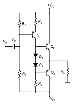
Figure \(\PageIndex{18}\): Class B amplifier with direct coupled driver, PNP version.
References
1Think of a car engine: How much sense would it make to have an engine with a 6000 RPM maximum run at 3000 RPM when you're sitting motionless at a red light?
2Of course, the dynamic resistance is a function of the current flowing through the diode so it will fluctuate as the signal changes. This is best thought of as a distortion generating mechanism because it will slightly alter the signal that reaches the base. This distortion is most likely orders of magnitude smaller than the notch distortion the diode mitigates, so it's a good trade.