
12.8: Exercises
- Page ID
- 34254

12.8.1: Analysis Problems
1. For the circuit of Figure \(\PageIndex{1}\), determine \(I_D\), \(V_G\) and \(V_D\). \(I_{DSS}\) = 20 mA, \(V_{GS(off)}\) = −6 V, \(V_{DD}\) = 15 V, \(R_G\) = 470 k\(\Omega\), \(R_S\) = 1.2 k\(\Omega\), \(R_D\) = 1.8 k\(\Omega\).
2. For the circuit of Figure \(\PageIndex{1}\), determine \(I_D\), \(V_{DS}\) and \(V_D\). \(I_{DSS}\) = 20 mA, \(V_{GS(off)}\) = −5 V, \(V_{DD}\) = 30 V, \(R_G\) = 560 k\(\Omega\), \(R_S\) = 420 \(\Omega\), \(R_D\) = 1.5 k\(\Omega\).
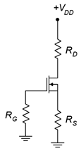
Figure \(\PageIndex{1}\)
3. For Figure \(\PageIndex{2}\), determine \(I_D\), \(V_G\) and \(V_D\). \(I_{DSS}\) = 15 mA, \(V_{DD}\) = 25 V, \(V_{GS(off)}\) = −3 V, \(V_{SS}\) = −6 V, \(R_G\) = 820 k\(\Omega\), \(R_S\) = 2 k\(\Omega\), \(R_D\) = 3.6 k\(\Omega\).
4. For the circuit of Figure \(\PageIndex{2}\), determine \(I_D\), \(V_{DS}\) and \(V_D\). \(I_{DSS}\) = 18 mA, \(V_{GS(off)}\) = −3 V, \(V_{DD}\) = 30 V, \(V_{SS}\) = −9 V, \(R_G\) = 910 k\(\Omega\), \(R_S\) = 1.2 k\(\Omega\), \(R_D\) = 2.7 k\(\Omega\).
5. For the circuit of Figure \(\PageIndex{3}\), determine \(I_D\), \(V_G\) and \(V_D\). \(I_{DSS}\) = 12 mA, \(V_{GS(off)}\) = −4 V, \(V_{DD}\) = 35 V, \(R_G\) = 680 k\(\Omega\), \(R_D\) = 1.8 k\(\Omega\).
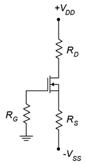
Figure \(\PageIndex{2}\)
6. For the circuit of Figure \(\PageIndex{3}\), determine \(I_D\), \(V_{DS}\) and \(V_D\). \(I_{DSS}\) = 8 mA, \(V_{GS(off)}\) = −2 V, \(V_{DD}\) = 30 V, \(R_G\) = 750 k\(\Omega\), \(R_D\) = 2.7 k\(\Omega\).
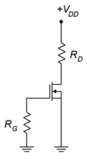
Figure \(\PageIndex{3}\)
7. For the circuit of Figure \(\PageIndex{4}\), determine \(I_D\), \(V_G\) and \(V_D\). \(I_{DSS}\) = 8 mA, \(V_{GS(off)}\) = −4 V, \(V_{DD}\) = 30 V, \(R_1\) = 2.7 M\(\Omega\), \(R_2\) = 110 k\(\Omega\), \(R_D\) = 470 \(\Omega\).
8. For the circuit of Figure \(\PageIndex{4}\), determine \(I_D\), \(V_{DS}\) and \(V_D\). \(I_{DSS}\) = 12 mA, \(V_{GS(off)}\) = −6 V, \(V_{DD}\) = 20 V, \(R_1\) = 2 M\(\Omega\), \(R_2\) = 100 k\(\Omega\), \(R_D\) = 680 \(\Omega\).
9. For the circuit of Figure \(\PageIndex{5}\), determine \(I_D\), \(V_G\) and \(V_D\). \(I_{D(on)}\) = 8 mA, \(V_{GS(on)}\) = 5 V, \(V_{GS(th)}\) = 3 V, \(V_{DD}\) = 30 V, \(R_1\) = 2 M\(\Omega\), \(R_2\) = 330 k\(\Omega\), \(R_D\) = 1.2 k\(\Omega\).
10. For the circuit of Figure \(\PageIndex{5}\), determine \(I_D\), \(V_{DS}\) and \(V_D\). \(I_{D(on)}\) = 12 mA, \(V_{GS(on)}\) = 6 V, \(V_{GS(th)}\) = 2.5 V, \(V_{DD}\) = 25 V, \(R_1\) = 1.5 M\(\Omega\), \(R_2\) = 470 k\(\Omega\), \(R_D\) = 680 \(\Omega\).
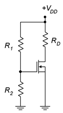
Figure \(\PageIndex{4}\)
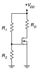
Figure \(\PageIndex{5}\)
11. For the circuit of Figure \(\PageIndex{6}\), determine \(I_D\), \(V_G\) and \(V_D\). \(I_{DSS}\) = 12 mA, \(V_{GS(off)}\) = 2 V, \(V_{DD}\) = −25 V, \(R_G\) = 470 k\(\Omega\), \(R_S\) = 800 \(\Omega\), \(R_D\) = 1.8 k\(\Omega\).
12. For the circuit of Figure \(\PageIndex{6}\), determine \(I_D\) and \(V_D\). \(I_{DSS}\) = 10 mA, \(V_{GS(off)}\) = 2 V, \(V_{DD}\) = −20 V, \(R_G\) = 560 k\(\Omega\), \(R_S\) = 680 \(\Omega\), \(R_D\) = 1.5 k\(\Omega\).
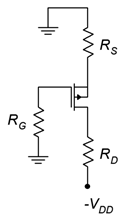
Figure \(\PageIndex{6}\)
13. For the circuit of Figure \(\PageIndex{7}\), determine \(I_D\), \(V_G\) and \(V_D\). \(I_{DSS}\) = 14 mA, \(V_{GS(off)}\) = 3 V, \(V_{DD}\) = −25 V, \(V_{SS}\) = 6 V, \(R_G\) = 780 k\(\Omega\), \(R_S\) = 2 k\(\Omega\), \(R_D\) = 3.3 k\(\Omega\).
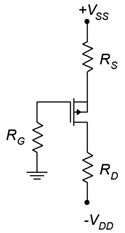
Figure \(\PageIndex{7}\)
14. For the circuit of Figure \(\PageIndex{7}\), determine \(I_D\) and \(V_D\). \(I_{DSS}\) = 16 mA, \(V_{GS(off)}\) = 3.5 V, \(V_{DD}\) = −20 V, \(V_{SS}\) = 7 V, \(R_G\) = 1 M\(\Omega\), \(R_S\) = 1.5 k\(\Omega\), \(R_D\) = 2.2 k\(\Omega\).
15. For the circuit of Figure \(\PageIndex{8}\), determine \(I_D\) and \(V_D\). \(I_{DSS}\) = 11 mA, \(V_{GS(off)}\) = 2 V, \(V_{DD}\) = −24 V, \(R_G\) = 750 k\(\Omega\), \(R_D\) = 1.2 k\(\Omega\).
16. For the circuit of Figure \(\PageIndex{8}\), determine \(I_D\) and \(V_D\). \(I_{DSS}\) = 9 mA, \(V_{GS(off)}\) = 3 V, \(V_{DD}\) = −18 V, \(R_G\) = 430 k\(\Omega\), \(R_D\) = 910 \(\Omega\).
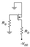
Figure \(\PageIndex{8}\)
12.8.2: Design Problems
17. Using the circuit of Figure \(\PageIndex{1}\), determine a value for \(R_S\) to set \(I_D\) to 4 mA. \(I_{DSS}\) = 10 mA, \(V_{GS(off)}\) = −2 V, \(V_{DD}\) = 18 V, \(R_G\) = 470 k\(\Omega\), \(R_D\) = 1.5 k\(\Omega\).
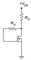
Figure \(\PageIndex{9}\)
18. For the circuit of Figure \(\PageIndex{9}\), determine \(R_D\) and \(R_G\) to set \(I_D\) = 10 mA. \(I_{D(on)}\) = 15 mA, \(V_{GS(on)}\) = 6 V, \(V_{GS(th)}\) = 2 V, \(V_{DD}\) = 20 V.
19. For the circuit of Figure \(\PageIndex{9}\), determine \(R_D\) and \(R_G\) to set \(I_D\) = 15 mA. \(I_{D(on)}\) = 10 mA, \(V_{GS(on)}\) = 5 V, \(V_{GS(th)}\) = 2 V, \(V_{DD}\) = 25 V.
12.8.3: Challenge Problems
20. Using the circuit of Figure \(\PageIndex{2}\), determine values for \(R_D\), \(R_S\) and \(V_{SS}\) to set \(I_D\) to 5 mA and \(V_D\) to 20 V. \(I_{DSS}\) = 15 mA, \(V_{GS(off)}\) = −3 V, \(V_{DD}\) = 30 V, \(R_G\) = 560 k\(\Omega\).
21. Using the circuit of Figure \(\PageIndex{10}\), determine values for \(R_D\) to set \(V_D\) to 15 V. \(I_{DSS}\) = 10 mA, \(V_{GS(off)}\) = 3 V, \(V_{SS}\) = 25 V, \(R_G\) = 680 k\(\Omega\).
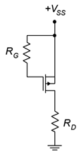
Figure \(\PageIndex{10}\)
Figure \(\PageIndex{11}\): Comic courtesy of xkcd.com