
3.3.6: Forward Biased
- Page ID
- 89953

Now let's take a look at what happens when we apply an external voltage to this junction. First we need some conventions. We make connections to the device using contacts, which we show as cross-hatched blocks. These contacts allow the free passage of current into and out of the device. Current usually flows through wires in the form of electrons, so it is easy to imagine electrons flowing into or out of the n-region. In the p-region, when electrons flow out of the device into the wire, holes will flow into the p-region (so as to maintain continuity of current through the contact.) When electrons flow into the p-region, they will recombine with holes, and so we have the net effect of holes flowing out of the p-region.
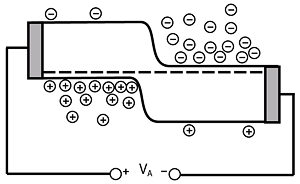
With the convention that a positive applied voltage means that the terminal connected to the p-region is positive with respect to the terminal connected to the n-region. This is easy to remember: "p is positive, n is negative". Let us try to figure out what will happen when we apply a positive applied voltage \(V_{a}\). If \(V_{a}\) is positive, then that means that the potential energy for electrons on the p-side must be lower than it was under the equilibrium condition. We reflect this on the band diagram by lowering the bands on the p-side from where they were originally. This is shown in Figure \(\PageIndex{2}\).
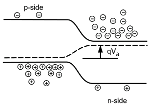
As we can see from Figure \(\PageIndex{2}\), when the p-region is lowered a couple of things happen. First of all, the Fermi level (the dotted line) is no longer a flat line, but rather it bends upward in going from the p-region to the n-region. This bending of the Fermi level happens because applying a voltage to the device throws the device out of equilibrium--this situation is non-equilibrium, and the Fermi level is not constant. The amount it bends (and hence the amount of shift of the bands) is just given by \(q V_{a}\), where the energy scale we are using for the band diagram is in electron-volts which, as we said before, is a common measure of potential energy when we are talking about electronic materials. The other thing we can notice is that the electrons on the n-side and the holes on the p-side now "see" a lower potential energy barrier than they saw when no voltage was applied. In fact, it looks as if a lot of electrons now have sufficient energy such that they could move across from the n-region and flow into the p-region. Likewise, we would expect to see holes moving across from the p-region into the n-region.
This flow of carriers across the junction will result in a current flow across the junction. In order to see how this current will behave with applied voltage, we have to use a result from statistical thermodynamics concerning the distribution of electrons in the conduction band, and holes in the valence band . We saw from our "cups" analogy, that the electrons tend to fill in the lowest states first, with fewer and fewer of them as we go up in energy. For most situations, a very good description of just how the electrons are distributed in energy is given by a simple exponential decay. (This comes about from a statistical analysis of electrons, which belong to a class of particles called Fermions. Fermions have the properties that they are: a) indistinguishable from one another; b) obey the Pauli Exclusion Principle, which says that two Fermions can not occupy the same exact state (energy and spin); and c) remain at some fixed total number \(N\).)
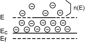
If \(n(E)\) tells us how many electrons there are with an energy greater than some value \(E_{c}\), then \(n(E)\) is given simply as: \[n(E) = N_{d} e^{- \frac{E-E_{c}}{kT}} \nonumber \]
The expression in the denominator is just Boltzmann's constant times the temperature in Kelvins. At room temperature \(kT\) has a value of about \(1/40\) of an \(\text{eV}\) or \(25 \mathrm{~meV}\). This number is sometimes called the thermal voltage, \(V_{T}\), but it's ok for you to just think of it as a constant which comes from the thermodynamics of the problem. Because \(kT \simeq 1/40\), you will sometimes see Equation \(\PageIndex{1}\) and similar equations written as \[n(E) = N_{d} e^{-40 \left(E-E_{c}\right)} \nonumber \]
This can look a little strange if you forget where the \(40\) came from, and just see it sitting there.
If the energy \(E\) is \(E_{c}\), the energy level of the conduction band, then \(n \left(E_{c}\right) = N_{d}\), the density of electrons in the n-type material. As \(E\) increases above \(E_{c}\), the density of electrons falls off exponentially, as depicted schematically in Figure \(\PageIndex{3}\):
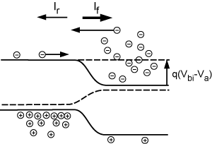
Now let's go back to the unbiased junction. Remember, as we said before, there are currents flowing across the junction, even if there is no bias. Of course without a bias voltage, the device is at equilibrium, the Fermi level is constant, and although current flows in the device, there is no net current flow. The current we have shown as \(I_{f}\) is due to those electrons which have an energy greater than the built-in potential. They are moving from right to left, as shown by the open arrow, which, of course, gives a current flowing from left to right, as shown by the solid arrows. Based on Equation \(\PageIndex{1}\) the current should be proportional to: \[I_{f} \propto N_{d} e^{- \frac{q V_{\text{bi}}}{kT}} \nonumber \]
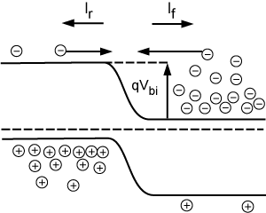
The principle of detailed balance says that at zero bias, \(I_{f} = -I_{r}\) and so \[I_{r} \propto - \left(N_{d} e^{- \frac{q V_{\text{bi}}}{kT}}\right) \nonumber \] \[I_{r} = \left( - \left(I_{f} \alpha \right)\right) - N_{d} e^{- \frac{q V_{\text{bi}}}{kT}} \nonumber \] That is to say, there is no net current flow in equlibrium.
Now, what happens when we apply the bias? For the electrons over on the n-side, the barrier has been reduced from a height of \(q V_{\text{bi}}\) to \(q \left(V_{\text{bi}} - V_{a}\right)\) and hence the forward current will be significantly increased. \[I_{f} \propto N_{d} e^{- \frac{q V_{\text{bi}}}{kT}} \nonumber \]
The reverse current, however, will remain just the same as it was before.
The total current across the junction is just \[\left(I_{f} + I_{r}\right) \propto N_{d} \left(e^{- \frac{q V_{a}}{kT}} - 1\right) \nonumber \]
where we have factored out the \(N_{d} e^{- \frac{q V_{\text{bi}}}{kT}}\) term out of both expressions. We are not prepared, with what we know at this point, to get the other terms in the proportionality that are involved here. Also, the astute reader will note that we have not said anything about the holes, but it should be obvious that they will also contribute to the current, and the arguments we have made for electrons will hold for the holes just as well.
We can take the effect of the holes, and the other unknowns about the proportionality, and bind them all into one constant called \(I_{\text{sat}}\) so that we write: \[I = I_{\text{sat}} \left(e^{\frac{q V_{a}}{kT}} - 1\right) \nonumber \]
This is the famous diode equation and is a very important result.
The Saturation Constant, often called a Scale current, is determined by the details of how the device is manufactured, and also by the temperature of the pn junction itself. Manufacturers usually give enough information in the data sheet that you can work out the constant for your needs.