3.3.8: Reverse Biased/Breakdown
- Page ID
- 89955

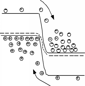
Before we leave diodes, it would be worthwhile exploring some other modes of operation, as well as some specific applications which will be of interest. We said that when the diode was reverse-biased (p-region negative with respect to the n-region) that the only current which flows is the reverse saturation current, resulting from the few thermally generated minority carriers which can fall down (or up) the barrier (Figure \(\PageIndex{1}\)).
If we make the reverse bias even greater, the same current flows, but the carriers pick up more energy as they fall down the (now larger) junction potential. As they do this, it is possible for them to pick up so much energy, that when they collide with a lattice site, they create an additional electron-hole pair through a process called impact ionization (Figure \(\PageIndex{2}\)). When this occurs, we now have current consisting of two electrons and one hole. These additional carriers can themselves collide and generate additional electron hole pairs as well. The current now consists of five electrons and two holes. This process is called avalanche multiplication (Figure \(\PageIndex{3}\)), because we start with one carrier, and through a succession of impacts create more and more current. This process can in fact run away, much like an avalanche on a snowy mountain side, in a process called avalanche breakdown.
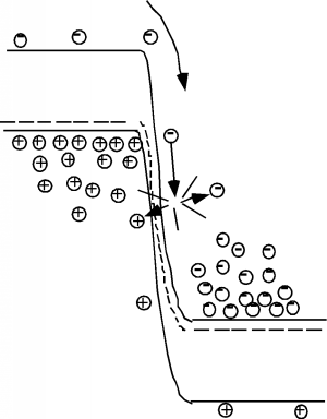
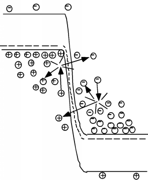 Figure \(\PageIndex{3}\): Avalanche multiplication
The net effect is to change the reverse characteristics of the diode somewhat. If we include the effect of breakdown in the I-V curve for the diode, we would see something like that in Figure \(\PageIndex{4}\).
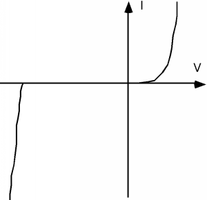
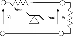
There is now a sudden onset of current after the avalanche breakdown voltage has been exceeded. Do not be confused into thinking that this "breakdown" means that the diode has been damaged. The process of avalanching itself is not destructive. But as you can see from Figure \(\PageIndex{4}\), the diode current increases very rapidly once the breakdown threshold has been exceeded. Thus, if there is not something in series with the diode to limit the maximum current through it, it could be damaged by overheating. Diodes in breakdown are used as voltage references (the voltage across them is more or less independent of the current running through them) but you will always find a series current limiting resistor used along with them. Such diodes are called Zener Diodes, the manufacturer can build diodes with a wide range of well-controlled breakdown voltages. The Zener Effect is also a reverse breakdown phenomena, but comes from direct field generation of extra carriers, rather than as a result of impact ionization. In truth, you can not tell the one effect from the other by looking at the diode I-V curve, and so all diodes used in reverse breakdown are called Zener Diodes. A circuit using a Zener diode as a voltage reference is shown in Figure \(\PageIndex{5}\).