
9.5.6: Photolithography
- Page ID
- 89986

Actually, implants (especially for moats) are usually done at a sufficiently high energy so that the dopant (phosphorus) is already pretty far into the substrate (often several microns or so), even before the diffusion starts. The anneal/diffusion moves the impurities into the wafer a bit more, and as we shall see also makes the n-region grow larger.
"The n-region"! We have not said a thing about how we make our moat in only certain areas of the wafer. From the description we have so far, it seems we have simply built an n-type layer over the whole surface of the wafer. This would be bad! We need to come up with some kind of "window" to only permit the implanting impurities to enter the silicon wafer where we want them and not elsewhere. We will do this by constructing an implantation "barrier".
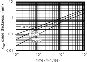
To do this, the first thing we do is grow a layer of silicon dioxide over the entire surface of the wafer. We talked about oxide growth when we were discussing MOSFETs, but let's go into a little more detail. You can grow oxide in either a dry oxygen atmosphere, or in a an atmosphere which contains water vapor, or steam. In Figure \(\PageIndex{1}\), we show oxide thickness as a function of time for growth with steam. Dry \(O_{2}\) does not behave too much differently; the rate is just somewhat slower.
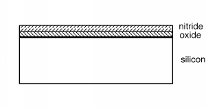
On top of the oxide, we are now going to deposit yet another material. This is silicon nitride, \(\mathrm{Si}_{3} \mathrm{N}_{4}\), usually just called plain "nitride". Silicon nitride is deposited through a method called chemical vapor deposition or "CVD". The usual technique is to react dichlorosilane and ammonia in a hot-walled low-pressure chemical vapor deposition system (LPCVD). The reaction is: \[3 \left(\mathrm{Si}, \mathrm{H}_{2}, \mathrm{Cl}_{2}\right) + 10 \left(\mathrm{N}, \mathrm{H}_{3}\right) \rightarrow \mathrm{Si}_{3} \left(\mathrm{N}_{4}\right) + 6 \left(\mathrm{N}, \mathrm{H}_{4}, \mathrm{Cl}\right) + 6 \left(\mathrm{H}_{2}\right)\]
Silicon nitride is a good barrier for impurities, oxygen and other things which we do not want to get into the wafer. Take a look at Figure \(\PageIndex{2}\) and see what we have so far. A word about scale and dimensions. The silicon wafer is about \(250 \ \mu\mathrm{m}\) thick (about 0.01"), since it has to be strong enough not to break as it is being handled. The two deposited layers are each about \(1 \ \mu\mathrm{m}\) thick, so they should actually be drawn as lines thinner than the other lines in the figure. This would obviously make the whole idea of a sketch ridiculous, so we will leave things distorted as they are, keeping in mind that the deposited and diffused layers are actually much thinner than the rest of the wafer, which really does not do anything except support the active circuits up on top. (There we go again, wasting silicon. Good thing it's cheap and plentiful!)
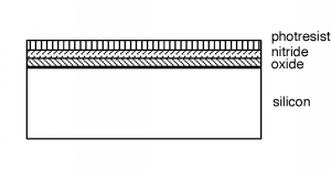
Now what we want to do is remove part of the nitride, so we can make our n-well, but not put in phosphorous where do not want it. We do this with processes called photolithography and etching, respectively. The first thing we do is coat the wafer with yet another layer of material. This is a liquid called photoresist and it is applied through a process called spin-coating. The wafer is put on a vacuum chuck, and a layer of liquid photoresist is sprayed on top of the wafer. The chuck is then spun rapidly, getting to several thousand RPM in a small fraction of a second. Centrifugal force causes the resist to spread out uniformly across the wafer surface (most of it, in fact, flies off!). The solvent for the photoresist is quite volatile and so the layer of photoresist dries while the wafer is still spinning, resulting in a thin, uniform coating across the wafer as shown in Figure \(\PageIndex{3}\).
The name "photoresist" gives some clue as to what this stuff is. Basically, photoresist is a polymer mixed with some kind of light sensitizing compound. In positive photoresist, wherever light strikes it, the polymer is weakened, and it can be more easily removed with a solvent during the development process. Conversely, negative photoresist is strengthened when it is illuminated with light, and is more resistant to the solvent than is the unilluminated photoresist. Positive resist is so-called because the image of the developed photoresist on the wafer looks just like the mask that was used to create it. Negative photoresist makes an image which is the opposite of what the mask looks like.
We have to come up with some way of selectively illuminating certain portions of the photoresist. Anyone who has ever seen a projector know how we can do this. But, since we want to make small things, not big ones, we will change around our projector so that it makes a smaller image, instead of a bigger one. The instrument that projects the light onto the photoresist on the wafer is called a projection printer or a stepper (Figure \(\PageIndex{4}\)).
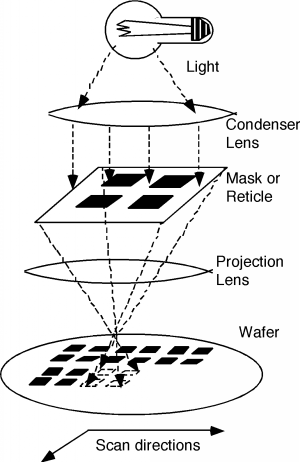
As shown in Figure \(\PageIndex{4}\), the stepper consists of several parts. There is a light source (usually a mercury vapor lamp, although ultra-violet excimer lasers are also starting to come into use), and a condenser lens to image the light source on the mask or reticle. The mask contains an image of the pattern we are trying to place on the wafer. The projection lens then makes a reduced (usually by 5x) image of the mask on the wafer. Because it would be far too costly, if not just plain impossible, to project onto the whole wafer all at once, only a small selected area is printed at one time. Then the wafer is scanned or stepped into a new position, and the image is printed again. If previous patterns have already been formed on the wafer, TV cameras with artificial intelligence algorithms are used to align the current image with the previously formed features. The stepper moves the whole surface of the wafer under the lens, until the wafer is completely covered with the desired pattern. A stepper is not cheap. Usually, TI or Intel will fork over several million dollars for each one! It is one of the most important pieces of equipment in the whole IC fab, however, since it determines what the minimum feature size on the circuit will be.
After exposure, the photoresist is placed in a suitable solvent, and "developed". Suppose for our example that the structure shown in Figure \(\PageIndex{5}\) is what results from the photolithographic step.
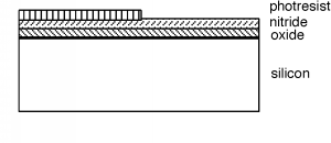
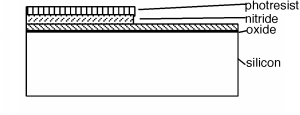
The pattern that was used in the photolithographic (PL) step exposed half of our area to light, and so the photoresist (PR) in that region was removed upon development. The wafer is now immersed in a hydrofluoric acid (HF) solution. HF acid etches silicon nitride quite rapidly, but does not etch silicon dioxide nearly as fast, so after the etch we have what we see in Figure \(\PageIndex{6}\).
We now take our wafer, put it in the ion implanter and subject it to a "blast" of phosphorus ions (see Figure \(\PageIndex{7}\)).
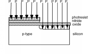
The ions go right through the oxide layer on the right hand side, but stick in the photoresist/nitride layer on the left half of our structure.