
2.3: Central Processing Unit
- Page ID
- 19864

\( \newcommand{\vecs}[1]{\overset { \scriptstyle \rightharpoonup} {\mathbf{#1}} } \)
\( \newcommand{\vecd}[1]{\overset{-\!-\!\rightharpoonup}{\vphantom{a}\smash {#1}}} \)
\( \newcommand{\dsum}{\displaystyle\sum\limits} \)
\( \newcommand{\dint}{\displaystyle\int\limits} \)
\( \newcommand{\dlim}{\displaystyle\lim\limits} \)
\( \newcommand{\id}{\mathrm{id}}\) \( \newcommand{\Span}{\mathrm{span}}\)
( \newcommand{\kernel}{\mathrm{null}\,}\) \( \newcommand{\range}{\mathrm{range}\,}\)
\( \newcommand{\RealPart}{\mathrm{Re}}\) \( \newcommand{\ImaginaryPart}{\mathrm{Im}}\)
\( \newcommand{\Argument}{\mathrm{Arg}}\) \( \newcommand{\norm}[1]{\| #1 \|}\)
\( \newcommand{\inner}[2]{\langle #1, #2 \rangle}\)
\( \newcommand{\Span}{\mathrm{span}}\)
\( \newcommand{\id}{\mathrm{id}}\)
\( \newcommand{\Span}{\mathrm{span}}\)
\( \newcommand{\kernel}{\mathrm{null}\,}\)
\( \newcommand{\range}{\mathrm{range}\,}\)
\( \newcommand{\RealPart}{\mathrm{Re}}\)
\( \newcommand{\ImaginaryPart}{\mathrm{Im}}\)
\( \newcommand{\Argument}{\mathrm{Arg}}\)
\( \newcommand{\norm}[1]{\| #1 \|}\)
\( \newcommand{\inner}[2]{\langle #1, #2 \rangle}\)
\( \newcommand{\Span}{\mathrm{span}}\) \( \newcommand{\AA}{\unicode[.8,0]{x212B}}\)
\( \newcommand{\vectorA}[1]{\vec{#1}} % arrow\)
\( \newcommand{\vectorAt}[1]{\vec{\text{#1}}} % arrow\)
\( \newcommand{\vectorB}[1]{\overset { \scriptstyle \rightharpoonup} {\mathbf{#1}} } \)
\( \newcommand{\vectorC}[1]{\textbf{#1}} \)
\( \newcommand{\vectorD}[1]{\overrightarrow{#1}} \)
\( \newcommand{\vectorDt}[1]{\overrightarrow{\text{#1}}} \)
\( \newcommand{\vectE}[1]{\overset{-\!-\!\rightharpoonup}{\vphantom{a}\smash{\mathbf {#1}}}} \)
\( \newcommand{\vecs}[1]{\overset { \scriptstyle \rightharpoonup} {\mathbf{#1}} } \)
\(\newcommand{\longvect}{\overrightarrow}\)
\( \newcommand{\vecd}[1]{\overset{-\!-\!\rightharpoonup}{\vphantom{a}\smash {#1}}} \)
\(\newcommand{\avec}{\mathbf a}\) \(\newcommand{\bvec}{\mathbf b}\) \(\newcommand{\cvec}{\mathbf c}\) \(\newcommand{\dvec}{\mathbf d}\) \(\newcommand{\dtil}{\widetilde{\mathbf d}}\) \(\newcommand{\evec}{\mathbf e}\) \(\newcommand{\fvec}{\mathbf f}\) \(\newcommand{\nvec}{\mathbf n}\) \(\newcommand{\pvec}{\mathbf p}\) \(\newcommand{\qvec}{\mathbf q}\) \(\newcommand{\svec}{\mathbf s}\) \(\newcommand{\tvec}{\mathbf t}\) \(\newcommand{\uvec}{\mathbf u}\) \(\newcommand{\vvec}{\mathbf v}\) \(\newcommand{\wvec}{\mathbf w}\) \(\newcommand{\xvec}{\mathbf x}\) \(\newcommand{\yvec}{\mathbf y}\) \(\newcommand{\zvec}{\mathbf z}\) \(\newcommand{\rvec}{\mathbf r}\) \(\newcommand{\mvec}{\mathbf m}\) \(\newcommand{\zerovec}{\mathbf 0}\) \(\newcommand{\onevec}{\mathbf 1}\) \(\newcommand{\real}{\mathbb R}\) \(\newcommand{\twovec}[2]{\left[\begin{array}{r}#1 \\ #2 \end{array}\right]}\) \(\newcommand{\ctwovec}[2]{\left[\begin{array}{c}#1 \\ #2 \end{array}\right]}\) \(\newcommand{\threevec}[3]{\left[\begin{array}{r}#1 \\ #2 \\ #3 \end{array}\right]}\) \(\newcommand{\cthreevec}[3]{\left[\begin{array}{c}#1 \\ #2 \\ #3 \end{array}\right]}\) \(\newcommand{\fourvec}[4]{\left[\begin{array}{r}#1 \\ #2 \\ #3 \\ #4 \end{array}\right]}\) \(\newcommand{\cfourvec}[4]{\left[\begin{array}{c}#1 \\ #2 \\ #3 \\ #4 \end{array}\right]}\) \(\newcommand{\fivevec}[5]{\left[\begin{array}{r}#1 \\ #2 \\ #3 \\ #4 \\ #5 \\ \end{array}\right]}\) \(\newcommand{\cfivevec}[5]{\left[\begin{array}{c}#1 \\ #2 \\ #3 \\ #4 \\ #5 \\ \end{array}\right]}\) \(\newcommand{\mattwo}[4]{\left[\begin{array}{rr}#1 \amp #2 \\ #3 \amp #4 \\ \end{array}\right]}\) \(\newcommand{\laspan}[1]{\text{Span}\{#1\}}\) \(\newcommand{\bcal}{\cal B}\) \(\newcommand{\ccal}{\cal C}\) \(\newcommand{\scal}{\cal S}\) \(\newcommand{\wcal}{\cal W}\) \(\newcommand{\ecal}{\cal E}\) \(\newcommand{\coords}[2]{\left\{#1\right\}_{#2}}\) \(\newcommand{\gray}[1]{\color{gray}{#1}}\) \(\newcommand{\lgray}[1]{\color{lightgray}{#1}}\) \(\newcommand{\rank}{\operatorname{rank}}\) \(\newcommand{\row}{\text{Row}}\) \(\newcommand{\col}{\text{Col}}\) \(\renewcommand{\row}{\text{Row}}\) \(\newcommand{\nul}{\text{Nul}}\) \(\newcommand{\var}{\text{Var}}\) \(\newcommand{\corr}{\text{corr}}\) \(\newcommand{\len}[1]{\left|#1\right|}\) \(\newcommand{\bbar}{\overline{\bvec}}\) \(\newcommand{\bhat}{\widehat{\bvec}}\) \(\newcommand{\bperp}{\bvec^\perp}\) \(\newcommand{\xhat}{\widehat{\xvec}}\) \(\newcommand{\vhat}{\widehat{\vvec}}\) \(\newcommand{\uhat}{\widehat{\uvec}}\) \(\newcommand{\what}{\widehat{\wvec}}\) \(\newcommand{\Sighat}{\widehat{\Sigma}}\) \(\newcommand{\lt}{<}\) \(\newcommand{\gt}{>}\) \(\newcommand{\amp}{&}\) \(\definecolor{fillinmathshade}{gray}{0.9}\)The Central Processing Unit (For more information, refer to: http://en.Wikipedia.org/wiki/Central_processing_unit) (CPU) is typically referred to as the “brains” of the computer since that is where the actual calculations are performed. The CPU is housed in a single chip, sometimes called a processor, chip, or die(For more information, refer to: http://en.Wikipedia.org/wiki/Die_(integrated_circuit)). The cover image shows one such CPU.
The CPU chip includes a number of functional units, including the Arithmetic Logic Unit(For more information, refer to: http://en.Wikipedia.org/wiki/Arithmetic_logic_unit) (ALU) which is the part of the chip that actually performs the arithmetic and logical calculations. In order to support the ALU, processor registers(For more information, refer to: http://en.Wikipedia.org/wiki/Processor_register) and cache(For more information, refer to: http://en.Wikipedia.org/wiki/Cache_(computing)) memory are also included “on the die” (term for inside the chip). The CPU registers and cache memory are described in subsequent sections.
It should be noted that the internal design of a modern processor is quite complex. This section provides a very simplified, high-level view of some key functional units within a CPU. Refer to the footnotes or additional references for more information.
Registers
A CPU register, or just register, is a temporary storage or working location built into the CPU itself (separate from memory). Computations are typically performed by the CPU using registers.
General Purpose Registers (GPRs)
There are sixteen, 64-bit General Purpose Registers (GPRs). The GPRs are described in the following table. A GPR register can be accessed with all 64-bits or some portion or subset accessed.
| 64-bit register | Lowest 32-bits | Lowest 16-bits | Lowest 8-bits |
|---|---|---|---|
| rax | eax | ax | a1 |
| rbx | ebx | bx | b1 |
| rcx | ecx | cx | c1 |
| rdx | edx | dx | d1 |
| rsi | esi | si | sil |
| rdi | edi | di | dil |
| rbp | ebp | bp | bp1 |
| rsp | esp | sp | sp1 |
| r8 | r8d | r8w | r8b |
| r9 | r9d | r9w | r9b |
| r10 | r10d | r10w | r10b |
| r11 | r11d | r11w | r11b |
| r12 | r12d | r12w | r12b |
| r13 | r13d | r13w | r13b |
| r14 | r14d | r14w | r14b |
| r15 | r15d | r15w | r15b |
Additionally, some of the GPR registers are used for dedicated purposes as described in the later sections.
When using data element sizes less than 64-bits (i.e., 32-bit, 16-bit, or 8-bit), the lower portion of the register can be accessed by using a different register name as shown in the table.
For example, when accessing the lower portions of the 64-bit rax register, the layout is as follows:
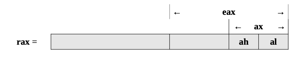
As shown in the diagram, the first four registers, rax, rbx, rcx, and rdx also allow the bits 8-15 to be accessed with the ah, bh, ch, and dh register names. With the exception of ah, these are provided for legacy support and will not be used in this text.
The ability to access portions of the register means that, if the quadword rax register is set to 50,000,000,00010 (fifty billion), the rax register would contain the following value in hex.
rax = 0000 000B A43B 7400
If a subsequent operation sets the word ax register to 50,00010 (fifty thousand, which is C35016), the rax register would contain the following value in hex.
rax = 0000 000B A43B C350
In this case, when the lower 16-bit ax portion of the 64-bit rax register is set, the upper 48-bits are unaffected. Note the change in AX (from \(7400_{16}\) to C\(350_{16}\)).
If a subsequent operation sets the byte sized al register to \(50_{10}\) (fifty, which is \(32_{16}\)), the rax register would contain the following value in hex.
rax = 0000 000B A43B C332
When the lower 8-bit al portion of the 64-bit rax register is set, the upper 56-bits are unaffected. Note the change in AL (from 5016 to 3216).
For 32-bit register operations, the upper 32-bits is cleared (set to zero). Generally, this is not an issue since operations on 32-bit registers do not use the upper 32-bits of the register. For unsigned values, this can be useful to convert from 32-bits to 64-bits. However, this will not work for signed conversions from 32-bit to 64-bit values. Specifically, it will potentially provide incorrect results for negative values. Refer to Chapter 3, Data Representation for additional information regarding the representation of signed values.
Stack Pointer Register (RSP)
One of the CPU registers, rsp, is used to point to the current top of the stack. The rsp register should not be used for data or other uses. Additional information regarding the stack and stack operations is provided in Chapter 9, Process Stack.
Pointer Register (RBP)
One of the CPU registers, rbp, is used as a base pointer during function calls. The rbp register should not be used for data or other uses. Additional information regarding the functions and function calls is provided in Chapter 12, Functions.
Instruction Pointer Register (RIP)
In addition to the GPRs, there is a special register, rip, which is used by the CPU to point to the next instruction to be executed. Specifically, since the rip points to the next instruction, that means the instruction being pointed to by rip, and shown in the debugger, has not yet been executed. This is an important distinction which can be confusing when reviewing code in a debugger.
Register (rFlags)
The flag register, rFlags, is used for status and CPU control information. The rFlag register is updated by the CPU after each instruction and not directly accessible by programs. This register stores status information about the instruction that was just executed. Of the 64-bits in the rFlag register, many are reserved for future use.
The following table shows some of the status bits in the flag register.
| Name | Symbol | Bit | Use |
|---|---|---|---|
| Carry | CF | 0 | Used to indicate if the previous operation resulted in a carry. |
| Parity | PF | 2 | Used to indicate if the last byte has an even number of 1's (i.e., even parity). |
| Adjust | AF | 4 | Used to support Binary Coded Decimal operations. |
| Zero | ZF | 6 | Used to indicate if the previous operation resulted in a zero result. |
| Sign | SF | 7 | Used to indicate if the result of the previous operation resulted in a 1 in the most significant bit (indicating negative in the context of signed data). |
| Direction | DF | 10 | Used to specify the direction (increment or decrement) for some string operations. |
| Overflow | OF | 11 | Used to indicate if the previous operation resulted in an overflow. |
There are a number of additional bits not specified in this text. More information can be obtained from the additional references noted in Chapter 1, Introduction.
Registers
There are a set of dedicated registers used to support 64-bit and 32-bit floating-point operations and Single Instruction Multiple Data (SIMD) instructions. The SIMD instructions allow a single instruction to be applied simultaneously to multiple data items. Used effectively, this can result in a significant performance increase. Typical applications include some graphics processing and digital signal processing.
The XMM registers as follows:
| 128-bit Registers |
| xmm0 |
| xmm1 |
| xmm2 |
| xmm3 |
| xmm4 |
| xmm5 |
| xmm6 |
| xmm7 |
| xmm8 |
| xmm9 |
| xmm10 |
| xmm11 |
| xmm12 |
| xmm13 |
| xmm14 |
| xmm15 |
Note, some of the more recent X86-64 processors support 256-bit XMM registers. This will not be an issue for the programs in this text.
Additionally, the XMM registers are used to support the Streaming SIMD Extensions (SSE). The SSE instructions are out of the scope of this text. More information can be obtained from the Intel references (as noted in Chapter 1, Introduction).
Cache Memory
Cache memory is a small subset of the primary storage or RAM located in the CPU chip. If a memory location is accessed, a copy of the value is placed in the cache. Subsequent accesses to that memory location that occur in quick succession are retrieved from the cache location (internal to the CPU chip). A memory read involves sending the address via the bus to the memory controller, which will obtain the value at the requested memory location, and send it back through the bus. Comparatively, if a value is in cache, it would be much faster to access that value.
A cache hit occurs when the requested data can be found in a cache, while a cache miss occurs when it cannot. Cache hits are served by reading data from the cache, which is faster than reading from main memory. The more requests that can be served from cache, the faster the system will typically perform. Successive generations of CPU chips have increased cache memory and improved cache mapping strategies in order to improve overall performance.
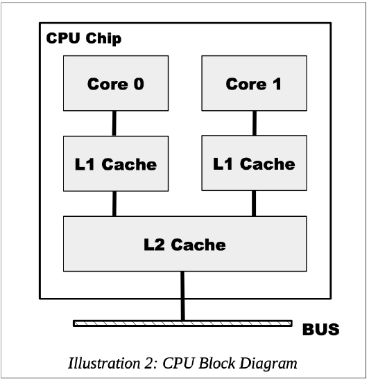
Current chip designs typically include an L1 cache per core and a shared L2 cache. Many of the newer CPU chips will have an additional L3 cache.
As can be noted from the diagram, all memory accesses travel through each level of cache. As such, there is a potential for multiple, duplicate copies of the value (CPU register, L1 cache, L2 cache, and main memory). This complication is managed by the CPU and is not something the programmer can change. Understanding the cache and associated performance gain is useful in understanding how a computer works.