
6.4: pn Junctions
- Page ID
- 18975

\( \newcommand{\vecs}[1]{\overset { \scriptstyle \rightharpoonup} {\mathbf{#1}} } \)
\( \newcommand{\vecd}[1]{\overset{-\!-\!\rightharpoonup}{\vphantom{a}\smash {#1}}} \)
\( \newcommand{\dsum}{\displaystyle\sum\limits} \)
\( \newcommand{\dint}{\displaystyle\int\limits} \)
\( \newcommand{\dlim}{\displaystyle\lim\limits} \)
\( \newcommand{\id}{\mathrm{id}}\) \( \newcommand{\Span}{\mathrm{span}}\)
( \newcommand{\kernel}{\mathrm{null}\,}\) \( \newcommand{\range}{\mathrm{range}\,}\)
\( \newcommand{\RealPart}{\mathrm{Re}}\) \( \newcommand{\ImaginaryPart}{\mathrm{Im}}\)
\( \newcommand{\Argument}{\mathrm{Arg}}\) \( \newcommand{\norm}[1]{\| #1 \|}\)
\( \newcommand{\inner}[2]{\langle #1, #2 \rangle}\)
\( \newcommand{\Span}{\mathrm{span}}\)
\( \newcommand{\id}{\mathrm{id}}\)
\( \newcommand{\Span}{\mathrm{span}}\)
\( \newcommand{\kernel}{\mathrm{null}\,}\)
\( \newcommand{\range}{\mathrm{range}\,}\)
\( \newcommand{\RealPart}{\mathrm{Re}}\)
\( \newcommand{\ImaginaryPart}{\mathrm{Im}}\)
\( \newcommand{\Argument}{\mathrm{Arg}}\)
\( \newcommand{\norm}[1]{\| #1 \|}\)
\( \newcommand{\inner}[2]{\langle #1, #2 \rangle}\)
\( \newcommand{\Span}{\mathrm{span}}\) \( \newcommand{\AA}{\unicode[.8,0]{x212B}}\)
\( \newcommand{\vectorA}[1]{\vec{#1}} % arrow\)
\( \newcommand{\vectorAt}[1]{\vec{\text{#1}}} % arrow\)
\( \newcommand{\vectorB}[1]{\overset { \scriptstyle \rightharpoonup} {\mathbf{#1}} } \)
\( \newcommand{\vectorC}[1]{\textbf{#1}} \)
\( \newcommand{\vectorD}[1]{\overrightarrow{#1}} \)
\( \newcommand{\vectorDt}[1]{\overrightarrow{\text{#1}}} \)
\( \newcommand{\vectE}[1]{\overset{-\!-\!\rightharpoonup}{\vphantom{a}\smash{\mathbf {#1}}}} \)
\( \newcommand{\vecs}[1]{\overset { \scriptstyle \rightharpoonup} {\mathbf{#1}} } \)
\(\newcommand{\longvect}{\overrightarrow}\)
\( \newcommand{\vecd}[1]{\overset{-\!-\!\rightharpoonup}{\vphantom{a}\smash {#1}}} \)
\(\newcommand{\avec}{\mathbf a}\) \(\newcommand{\bvec}{\mathbf b}\) \(\newcommand{\cvec}{\mathbf c}\) \(\newcommand{\dvec}{\mathbf d}\) \(\newcommand{\dtil}{\widetilde{\mathbf d}}\) \(\newcommand{\evec}{\mathbf e}\) \(\newcommand{\fvec}{\mathbf f}\) \(\newcommand{\nvec}{\mathbf n}\) \(\newcommand{\pvec}{\mathbf p}\) \(\newcommand{\qvec}{\mathbf q}\) \(\newcommand{\svec}{\mathbf s}\) \(\newcommand{\tvec}{\mathbf t}\) \(\newcommand{\uvec}{\mathbf u}\) \(\newcommand{\vvec}{\mathbf v}\) \(\newcommand{\wvec}{\mathbf w}\) \(\newcommand{\xvec}{\mathbf x}\) \(\newcommand{\yvec}{\mathbf y}\) \(\newcommand{\zvec}{\mathbf z}\) \(\newcommand{\rvec}{\mathbf r}\) \(\newcommand{\mvec}{\mathbf m}\) \(\newcommand{\zerovec}{\mathbf 0}\) \(\newcommand{\onevec}{\mathbf 1}\) \(\newcommand{\real}{\mathbb R}\) \(\newcommand{\twovec}[2]{\left[\begin{array}{r}#1 \\ #2 \end{array}\right]}\) \(\newcommand{\ctwovec}[2]{\left[\begin{array}{c}#1 \\ #2 \end{array}\right]}\) \(\newcommand{\threevec}[3]{\left[\begin{array}{r}#1 \\ #2 \\ #3 \end{array}\right]}\) \(\newcommand{\cthreevec}[3]{\left[\begin{array}{c}#1 \\ #2 \\ #3 \end{array}\right]}\) \(\newcommand{\fourvec}[4]{\left[\begin{array}{r}#1 \\ #2 \\ #3 \\ #4 \end{array}\right]}\) \(\newcommand{\cfourvec}[4]{\left[\begin{array}{c}#1 \\ #2 \\ #3 \\ #4 \end{array}\right]}\) \(\newcommand{\fivevec}[5]{\left[\begin{array}{r}#1 \\ #2 \\ #3 \\ #4 \\ #5 \\ \end{array}\right]}\) \(\newcommand{\cfivevec}[5]{\left[\begin{array}{c}#1 \\ #2 \\ #3 \\ #4 \\ #5 \\ \end{array}\right]}\) \(\newcommand{\mattwo}[4]{\left[\begin{array}{rr}#1 \amp #2 \\ #3 \amp #4 \\ \end{array}\right]}\) \(\newcommand{\laspan}[1]{\text{Span}\{#1\}}\) \(\newcommand{\bcal}{\cal B}\) \(\newcommand{\ccal}{\cal C}\) \(\newcommand{\scal}{\cal S}\) \(\newcommand{\wcal}{\cal W}\) \(\newcommand{\ecal}{\cal E}\) \(\newcommand{\coords}[2]{\left\{#1\right\}_{#2}}\) \(\newcommand{\gray}[1]{\color{gray}{#1}}\) \(\newcommand{\lgray}[1]{\color{lightgray}{#1}}\) \(\newcommand{\rank}{\operatorname{rank}}\) \(\newcommand{\row}{\text{Row}}\) \(\newcommand{\col}{\text{Col}}\) \(\renewcommand{\row}{\text{Row}}\) \(\newcommand{\nul}{\text{Nul}}\) \(\newcommand{\var}{\text{Var}}\) \(\newcommand{\corr}{\text{corr}}\) \(\newcommand{\len}[1]{\left|#1\right|}\) \(\newcommand{\bbar}{\overline{\bvec}}\) \(\newcommand{\bhat}{\widehat{\bvec}}\) \(\newcommand{\bperp}{\bvec^\perp}\) \(\newcommand{\xhat}{\widehat{\xvec}}\) \(\newcommand{\vhat}{\widehat{\vvec}}\) \(\newcommand{\uhat}{\widehat{\uvec}}\) \(\newcommand{\what}{\widehat{\wvec}}\) \(\newcommand{\Sighat}{\widehat{\Sigma}}\) \(\newcommand{\lt}{<}\) \(\newcommand{\gt}{>}\) \(\newcommand{\amp}{&}\) \(\definecolor{fillinmathshade}{gray}{0.9}\)Many devices, including photovoltaic devices, LEDs, photodiodes, semiconductor lasers, and thermoelectric devices are essentially made from pn junctions. To understand photovoltaic devices and these other energy conversion devices, we need to understand pn junctions. Consider a semiconductor crystal composed of an n-type material (with excess electrons) on one side and a p-type material (lacking electrons, in other words, with an excess of holes) on the other side. The junction of the p-type and n-type materials is called a pn junction. Assume the junction is abrupt and is at thermal equilibrium.
Some pn junctions are made from elemental semiconductors like Si, and other pn junctions are made from compound semiconductors like GaAs.
Some pn junctions have the same material on both sides while other pn junctions have different materials on either side. For example, a pn junction can be made from an n-type layer of GaAs and a p-type layer of GaAs. It can also be made from an n-type layer of GaAs and a p-type layer of AlAs.
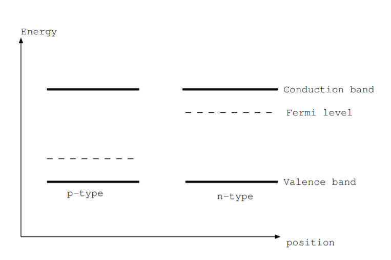
What happens when we put a p-type material and an n-type material together to form a pn junction? Valence electrons and holes move. Nuclei and inner shell electrons do not. Some excess electrons from the n-type region go towards the p-type region. Some excess holes from the p-type region go towards the n-type region. These charge carriers diffuse, are swept away from, a region near the junction. This region near the junction which is lacking charge carriers is called the depletion layer [10, p. 564]. As shown in Fig. \(\PageIndex{1}\), the Fermi level \(E_f\) is near the valence band for p-type materials. P-type material lacks electrons, so the energy where it is equally likely to find an electron state occupied and unoccupied is closer to the valence band. For a similar reason, the Fermi level \(E_f\) is near the conduction band for n-type materials. Figure \(\PageIndex{2}\) shows the energy level diagram versus position for the pn junction, and Fermi levels of the two materials are lined up in this figure.
Consider a junction where the n-type material is silicon doped with phosphorous atoms and the p-type material is silicon doped with aluminum atoms. The n-type side of the pn junction has an excess of positive charges because some phosphorous atoms replace Si atoms in the material. Phosphorous atoms have one more proton than silicon atoms. They also have one more electron, but the valence electron is a charge carrier which diffuses away from the junction. Similarly, the p-type side of the junction has an excess of negative charges because some aluminum atoms replace silicon atoms. Aluminum atoms have one less proton than Si atoms. They also have one less electron, but the hole is a charge carrier which also diffuses away from the junction.
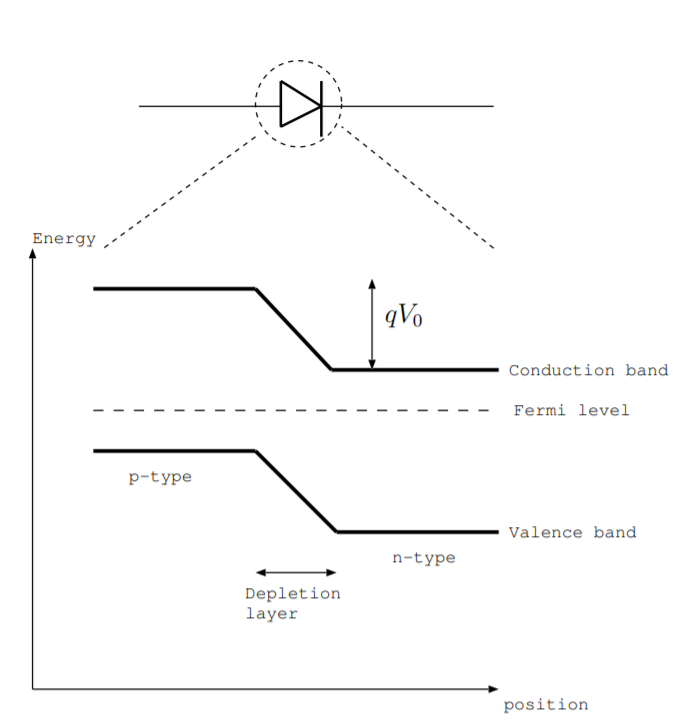
An electric field forms across the junction due to the net charge distribution near the junction. Electric field intensity is the force per unit charge, and it has the units \(\frac{V}{m}\). There is also necessarily a voltage drop across a pn junction in equilibrium, and this voltage is called the contact potential \(V_0\) in the units of volts. While the contact potential is a voltage, it cannot be measured by placing a voltmeter across a pn junction because additional junctions would be formed at each lead of the voltmeter with additional voltages introduced [9, p. 141].
Figure \(\PageIndex{2}\) illustrates the energy level diagram of a pn junction. The horizontal axis represents position, and the vertical axis represents energy. It is related to the figures in Section 6.2. However, Fig. \(\PageIndex{2}\) is zoomed in vertically, and it is plotted versus position near the junction. It also shows the relationship between the energy level diagram and the circuit symbol for a diode, and the depletion layer is labeled. The vertical distance \(qV_0\), also labeled in Fig. \(\PageIndex{2}\), represents the amount of energy required to move an electron across the junction [9, p. 141].
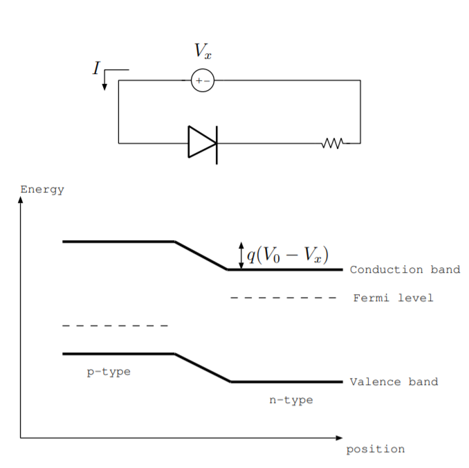
Figure \(\PageIndex{3}\) shows the energy level diagram for a forward biased pn junction. In a forward biased pn junction, current flows from the p-type to n-type side of the junction. More specifically, holes flow from the p-type to n-type region, and some of these holes neutralize excess charges in the depletion layer. The depletion layer becomes narrower. The electric field preventing the flow of charges gets smaller, and the voltage drop across the junction gets smaller. The energy \(q (V_0 - V_x)\) is labeled in Fig. \(\PageIndex{3}\) for a forward biased pn junction where the voltage \(V_x\) is the voltage supplied. This energy represents the energy needed to get charges to flow across the junction, and it is smaller than the corresponding energy in the case of the unbiased junction. Charges flow more easily in the case of a forward biased pn junction, and the diode acts as a wire.
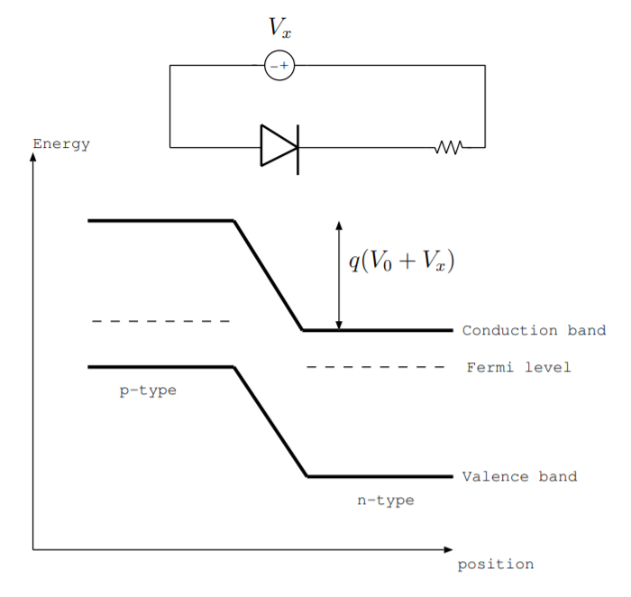
Figure \(\PageIndex{4}\) shows the energy level diagram for a reversed biased pn junction. For a reverse biased pn junction, the voltage across the junction \(V_0 + V_x\) is larger than for an unbiased junction, and the energy needed for charges to flow \(q (V_0 + V_x)\) is larger than for an unbiased junction. Reversed biased pn junctions act as open circuits, and charges do not flow due to this amount of energy required.
A light emitting diode (LED) is a device that converts electricity to optical electromagnetic energy, and it is made from a semiconductor pn junction. In use, a forward bias is put across the LED as shown in Fig. \(\PageIndex{3}\). Holes flow from the p-type to n-type region. Some of these holes combine with electrons in the depletion layer. In an LED, photons are emitted in this process. The energy of the emitted photon corresponds to the energy of the energy gap. Some LEDs have an additional intrinsic, undoped, layer at the junction, between the p-type and n-type layers to improve the efficiency of the device.
A solar cell and an optical photodetector are also essentially pn junctions. Both of these devices convert optical electromagnetic energy to electricity. When light shines on these devices, electron-hole pairs are created at the junction. Due to the charge distribution across the junction, many of the electrons and holes created are swept away from the junction before they can recombine [9]. This flow of charges is a current, so the optical electromagnetic energy is converted into electricity. When light shines on a photovoltaic device, a voltage can be measured across the junction, and this effect is called the photovoltaic effect [9, p. 212].
The vertical distance between the conduction band and the valence band on an energy level diagram is the energy gap \(E_g\). The energy gap of the material used to make a solar cell or photodetector determines the properties of the device. Photons with energy greater than the energy gap have enough energy to form electron-hole pairs while photons with less energy cannot.
If a temperature gradient is applied across a pn junction, charges flow. When one side of the device is heated, charges move more rapidly and these energetic charges diffuse to the cooler side. This effect, called the Seebeck thermoelectric effect, is discussed in Chapter 8.