
4.6: Exercises


- Last updated
- Jun 6, 2021
- Save as PDF

( \newcommand{\kernel}{\mathrm{null}\,}\)
Analysis
Assume the source's angle is 0 degrees unless specified otherwise.
1. Determine the impedance of the circuit of Figure 4.6.1 at frequencies of 100 Hz, 10 kHz and 1 MHz.
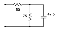
Figure 4.6.1
2. Determine the impedance of the circuit of Figure 4.6.2 at frequencies of 20 Hz, 1 kHz and 20 kHz.
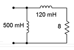
Figure 4.6.2
3. Determine the impedance of the circuit of Figure 4.6.3 at frequencies of 300 Hz, 30 kHz and 3 MHz.
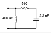
Figure 4.6.3
4. Determine the impedance of the circuit of Figure 4.6.4 at frequencies of 1 kHz, 20 kHz and 1 MHz.
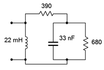
Figure 4.6.4
5. Determine the impedance of the circuit of Figure 4.6.5.
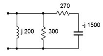
Figure 4.6.5
6. Determine the impedance of the circuit of Figure 4.6.6.
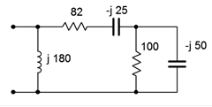
Figure 4.6.6
7. For the circuit of Figure 4.6.7, determine the source current and the current through each of the components.
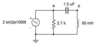
Figure 4.6.7
8. For the circuit of Figure 4.6.7, determine voltages vab and vb.
9. For the circuit of Figure 4.6.8, determine voltages across R, L and C if the source is 7 volts RMS.
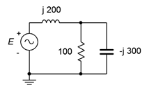
Figure 4.6.8
10. For the circuit of Figure 4.6.8, determine the source current and the current through each of the three components. Also, draw a phasor diagram of E, vL and vR.
11. For the circuit of Figure 4.6.9, determine the source current and the current through each of the components.
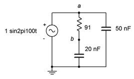
Figure 4.6.9
12. For the circuit of Figure 4.6.9, determine voltages vab and vb. Also, draw a phasor diagram of E, vab and vb.
13. For the circuit of Figure 4.6.10, determine voltages vab and vb if the source is 20 volts peak.
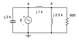
Figure 4.6.10
14. For the circuit of Figure 4.6.10, determine the source current and the current through each of the four components if the source is 20 volts peak.
15. For the circuit of Figure 4.6.11, determine the source current and the current through each of the four components.
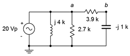
Figure 4.6.11
16. For the circuit of Figure 4.6.11, determine voltages vab and vb.
17. For the circuit of Figure 4.6.12, determine voltages vab and vb if the source is 100 volts peak.
18. For the circuit of Figure 4.6.12, determine the currents through the two resistors.
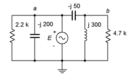
Figure 4.6.12
19. For the circuit of Figure 4.6.13, determine the currents each of the three components.
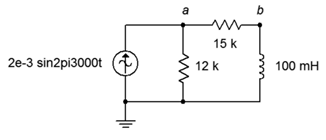
Figure 4.6.13
20. For the circuit of Figure 4.6.13, determine voltages va and vb.
21. For the circuit of Figure 4.6.14, determine voltages va and vb.
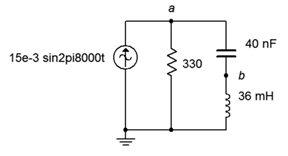
Figure 4.6.14
22. For the circuit of Figure 4.6.14, determine the middle and right branch currents and draw a phasor diagram of three circuit currents.
23. For the circuit of Figure 4.6.15, determine voltages va and vb.
24. For the circuit of Figure 4.6.15, determine the currents through the two resistors.
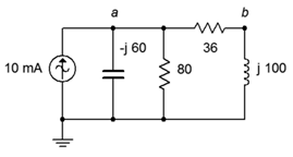
Figure 4.6.15
25. For the circuit of Figure 4.6.16, determine voltages va and vb. isource=25 mA.
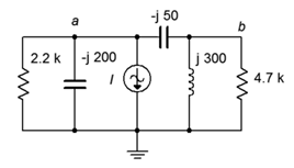
Figure 4.6.16
26. For the circuit of Figure 4.6.16, determine the currents through the two capacitors.
27. For the circuit of Figure 4.6.17, determine the current through the capacitor. i1=10E−3∠0∘A and i2=3E−3∠90∘A.
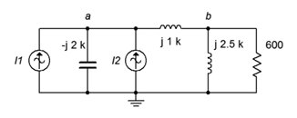
Figure 4.6.17
28. For the circuit of Figure 4.6.17, determine voltages va and vb. I1=10E−3∠0∘A and I2=3E−3∠90∘A.
29. For the circuit of Figure 4.6.18, determine voltages va and vb. i1=2∠45∘A and i2=0.5∠0∘A.
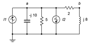
Figure 4.6.18
30. For the circuit of Figure 4.6.18, determine the currents through the two resistors. i1=2∠45∘A and i2=0.5∠0∘A.
31. For the bridge circuit of Figure 4.6.19, determine vab. The source is 50 volts peak.
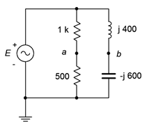
Figure 4.6.19
32. For the bridge circuit of Figure 4.6.20, determine vab. The source is 6 amps peak.
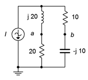
Figure 4.6.20
Design
33. Determine a new value for the capacitor in Figure 4.6.7 such that vb is 1.5 volts.
34. Determine the required inductive reactance in Figure 4.6.8 to shift the capacitor voltage to half of the source voltage.
35. Determine a new value for the 20 nF capacitor in Figure 4.6.9 such that the resistor current is 2 mA.
36. In the circuit of Figure 4.6.21, determine a value for L such that the magnitude of vb equals va/2 if the source frequency is 10 kHz, R = 2.7 kΩ and C = 10 nF.
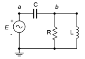
Figure 4.6.21
37. Given the circuit of Figure 4.6.21, determine a value for C such that the source current is in phase with the source voltage. The source frequency is 1 kHz, R = 68 Ω and L = 22 mH.
38. Given the circuit of Figure 4.6.22, determine a value for L such that vb is 1 volt. The source is a 6 volt peak sine at 50 kHz, R1 = 510 Ω and R2 = 220 Ω.
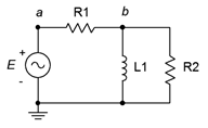
Figure 4.6.22
39. Given the circuit of Figure 4.6.19, determine a new value for the inductor such that the magnitude of vb equals the magnitude of va. Assume that the source frequency is 20 kHz.
Challenge
40. Consider the circuit drawn in Figure 4.6.23. Using only the available components of 1 kΩ, 2.2 kΩ, 1 mH, 5 mH, 10 nF, 75 nF and 560 nF, is it possible to configure a circuit such that va is half the magnitude of vb for a source frequency of 1 kHz? If so, indicate which values could be used for the four components. If not, explain your reasoning.
Figure 4.6.23
41. Given the circuit of Figure 4.6.9, determine the frequency at which vb is half of the source voltage.
42. For the circuit of Figure 4.6.24, determine voltages va, vb, and vc. i1=5∠0∘A and i2=3∠90∘A.
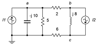
Figure 4.6.24
43. Given the circuit of Figure 4.6.19, is it possible to change the values of the two resistors such that the phase angle of va is the same as that of vb? If so, what are the new values, and if not, explain why it is not possible.
Simulation
44. Perform a transient analysis to verify the node voltages computed for problem 8.
45. Perform a transient analysis to verify the node voltages computed for problem 12.
46. Perform a transient analysis to verify the node voltages computed for problem 20.
47. Perform a transient analysis to verify the node voltages computed for problem 21.
48. Consider the circuit of problem 17. Assuming the source frequency is 10 kHz, determine values for the capacitors and inductors. Then, use a transient analysis to verify the results of problem 17.
49. Perform a transient analysis on the result of problem 33 to verify the accuracy of the design.
50. Perform a transient analysis on the result of problem 34 to verify the accuracy of the design.
51. Use an AC frequency response simulation to verify the results of problem 41.
52. The concept of a loudspeaker crossover network was presented originally in Chapter 2, Series RLC Circuits. In this chapter, we noted that by adding more components, it is possible to increase the rate of attenuation. In doing so the undesired signals are further reduced in amplitude. The circuits of Figure 4.6.25 and 4.6.26 (following page) show improved crossovers for a woofer and tweeter, respectively. Assuming standard 8 Ω loudspeakers, use an AC frequency domain simulation to determine the crossover frequency of each network. Also, compare the curves at node a to those at node b. Finally, compare the attenuation slopes to those generated by the simpler crossover network presented at the end of Chapter 2. Component values for the woofer: L1 = 760 μH, (L2\) = 250 μH, C = 10.6 μF. Component values for the tweeter: C1 = 5.3 μF, C2 = 16 μF, L = 380 μH.
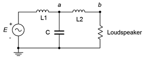
Figure 4.6.25
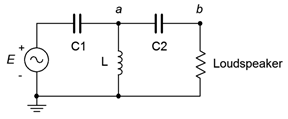
Figure 4.6.26