
10.6: Exercises
- Page ID
- 25317

\( \newcommand{\vecs}[1]{\overset { \scriptstyle \rightharpoonup} {\mathbf{#1}} } \)
\( \newcommand{\vecd}[1]{\overset{-\!-\!\rightharpoonup}{\vphantom{a}\smash {#1}}} \)
\( \newcommand{\dsum}{\displaystyle\sum\limits} \)
\( \newcommand{\dint}{\displaystyle\int\limits} \)
\( \newcommand{\dlim}{\displaystyle\lim\limits} \)
\( \newcommand{\id}{\mathrm{id}}\) \( \newcommand{\Span}{\mathrm{span}}\)
( \newcommand{\kernel}{\mathrm{null}\,}\) \( \newcommand{\range}{\mathrm{range}\,}\)
\( \newcommand{\RealPart}{\mathrm{Re}}\) \( \newcommand{\ImaginaryPart}{\mathrm{Im}}\)
\( \newcommand{\Argument}{\mathrm{Arg}}\) \( \newcommand{\norm}[1]{\| #1 \|}\)
\( \newcommand{\inner}[2]{\langle #1, #2 \rangle}\)
\( \newcommand{\Span}{\mathrm{span}}\)
\( \newcommand{\id}{\mathrm{id}}\)
\( \newcommand{\Span}{\mathrm{span}}\)
\( \newcommand{\kernel}{\mathrm{null}\,}\)
\( \newcommand{\range}{\mathrm{range}\,}\)
\( \newcommand{\RealPart}{\mathrm{Re}}\)
\( \newcommand{\ImaginaryPart}{\mathrm{Im}}\)
\( \newcommand{\Argument}{\mathrm{Arg}}\)
\( \newcommand{\norm}[1]{\| #1 \|}\)
\( \newcommand{\inner}[2]{\langle #1, #2 \rangle}\)
\( \newcommand{\Span}{\mathrm{span}}\) \( \newcommand{\AA}{\unicode[.8,0]{x212B}}\)
\( \newcommand{\vectorA}[1]{\vec{#1}} % arrow\)
\( \newcommand{\vectorAt}[1]{\vec{\text{#1}}} % arrow\)
\( \newcommand{\vectorB}[1]{\overset { \scriptstyle \rightharpoonup} {\mathbf{#1}} } \)
\( \newcommand{\vectorC}[1]{\textbf{#1}} \)
\( \newcommand{\vectorD}[1]{\overrightarrow{#1}} \)
\( \newcommand{\vectorDt}[1]{\overrightarrow{\text{#1}}} \)
\( \newcommand{\vectE}[1]{\overset{-\!-\!\rightharpoonup}{\vphantom{a}\smash{\mathbf {#1}}}} \)
\( \newcommand{\vecs}[1]{\overset { \scriptstyle \rightharpoonup} {\mathbf{#1}} } \)
\(\newcommand{\longvect}{\overrightarrow}\)
\( \newcommand{\vecd}[1]{\overset{-\!-\!\rightharpoonup}{\vphantom{a}\smash {#1}}} \)
\(\newcommand{\avec}{\mathbf a}\) \(\newcommand{\bvec}{\mathbf b}\) \(\newcommand{\cvec}{\mathbf c}\) \(\newcommand{\dvec}{\mathbf d}\) \(\newcommand{\dtil}{\widetilde{\mathbf d}}\) \(\newcommand{\evec}{\mathbf e}\) \(\newcommand{\fvec}{\mathbf f}\) \(\newcommand{\nvec}{\mathbf n}\) \(\newcommand{\pvec}{\mathbf p}\) \(\newcommand{\qvec}{\mathbf q}\) \(\newcommand{\svec}{\mathbf s}\) \(\newcommand{\tvec}{\mathbf t}\) \(\newcommand{\uvec}{\mathbf u}\) \(\newcommand{\vvec}{\mathbf v}\) \(\newcommand{\wvec}{\mathbf w}\) \(\newcommand{\xvec}{\mathbf x}\) \(\newcommand{\yvec}{\mathbf y}\) \(\newcommand{\zvec}{\mathbf z}\) \(\newcommand{\rvec}{\mathbf r}\) \(\newcommand{\mvec}{\mathbf m}\) \(\newcommand{\zerovec}{\mathbf 0}\) \(\newcommand{\onevec}{\mathbf 1}\) \(\newcommand{\real}{\mathbb R}\) \(\newcommand{\twovec}[2]{\left[\begin{array}{r}#1 \\ #2 \end{array}\right]}\) \(\newcommand{\ctwovec}[2]{\left[\begin{array}{c}#1 \\ #2 \end{array}\right]}\) \(\newcommand{\threevec}[3]{\left[\begin{array}{r}#1 \\ #2 \\ #3 \end{array}\right]}\) \(\newcommand{\cthreevec}[3]{\left[\begin{array}{c}#1 \\ #2 \\ #3 \end{array}\right]}\) \(\newcommand{\fourvec}[4]{\left[\begin{array}{r}#1 \\ #2 \\ #3 \\ #4 \end{array}\right]}\) \(\newcommand{\cfourvec}[4]{\left[\begin{array}{c}#1 \\ #2 \\ #3 \\ #4 \end{array}\right]}\) \(\newcommand{\fivevec}[5]{\left[\begin{array}{r}#1 \\ #2 \\ #3 \\ #4 \\ #5 \\ \end{array}\right]}\) \(\newcommand{\cfivevec}[5]{\left[\begin{array}{c}#1 \\ #2 \\ #3 \\ #4 \\ #5 \\ \end{array}\right]}\) \(\newcommand{\mattwo}[4]{\left[\begin{array}{rr}#1 \amp #2 \\ #3 \amp #4 \\ \end{array}\right]}\) \(\newcommand{\laspan}[1]{\text{Span}\{#1\}}\) \(\newcommand{\bcal}{\cal B}\) \(\newcommand{\ccal}{\cal C}\) \(\newcommand{\scal}{\cal S}\) \(\newcommand{\wcal}{\cal W}\) \(\newcommand{\ecal}{\cal E}\) \(\newcommand{\coords}[2]{\left\{#1\right\}_{#2}}\) \(\newcommand{\gray}[1]{\color{gray}{#1}}\) \(\newcommand{\lgray}[1]{\color{lightgray}{#1}}\) \(\newcommand{\rank}{\operatorname{rank}}\) \(\newcommand{\row}{\text{Row}}\) \(\newcommand{\col}{\text{Col}}\) \(\renewcommand{\row}{\text{Row}}\) \(\newcommand{\nul}{\text{Nul}}\) \(\newcommand{\var}{\text{Var}}\) \(\newcommand{\corr}{\text{corr}}\) \(\newcommand{\len}[1]{\left|#1\right|}\) \(\newcommand{\bbar}{\overline{\bvec}}\) \(\newcommand{\bhat}{\widehat{\bvec}}\) \(\newcommand{\bperp}{\bvec^\perp}\) \(\newcommand{\xhat}{\widehat{\xvec}}\) \(\newcommand{\vhat}{\widehat{\vvec}}\) \(\newcommand{\uhat}{\widehat{\uvec}}\) \(\newcommand{\what}{\widehat{\wvec}}\) \(\newcommand{\Sighat}{\widehat{\Sigma}}\) \(\newcommand{\lt}{<}\) \(\newcommand{\gt}{>}\) \(\newcommand{\amp}{&}\) \(\definecolor{fillinmathshade}{gray}{0.9}\)10.6.1: Analysis Problems
1. For the circuit of Figure \(\PageIndex{1}\), determine \(I_D\) and \(V_{DS}\). \(I_{DSS}\) = 40 mA, \(V_{GS(off)}\) = −4 V, \(V_{DD}\) = 26 V, \(V_{GG}\) = −2 V, \(R_G\) = 220 k\(\Omega\), \(R_D\) = 1.2 k\(\Omega\).
2. For the circuit of Figure \(\PageIndex{1}\), determine \(I_D\) and \(V_{DS}\). \(I_{DSS}\) = 20 mA, \(V_{GS(off)}\) = −3 V, \(V_{DD}\) = 22 V, \(V_{GG}\) = −1 V, \(R_G\) = 390 k\(\Omega\), \(R_D\) = 1 k\(\Omega\).
Figure \(\PageIndex{1}\)
3. For the circuit of Figure \(\PageIndex{2}\), determine \(I_D\), \(V_G\) and \(V_D\). \(I_{DSS}\) = 24 mA, \(V_{GS(off)}\) = −6 V, \(V_{DD}\) = 36 V, \(R_G\) = 220 k\(\Omega\), \(R_S\) = 2 k\(\Omega\), \(R_D\) = 1.8 k\(\Omega\).
4. For the circuit of Figure \(\PageIndex{2}\), determine \(I_D\), \(V_S\) and \(V_{DS}\). \(I_{DSS}\) = 18 mA, \(V_{GS(off)}\) = −3 V, \(V_{DD}\) = 30 V, \(R_G\) = 270 k\(\Omega\), \(R_S\) = 2.7 k\(\Omega\), \(R_D\) = 3.3 k\(\Omega\).
Figure \(\PageIndex{2}\)
5. For Figure \(\PageIndex{3}\), determine \(I_D\), \(V_G\) and \(V_D\). \(I_{DSS}\) = 16 mA, \(V_{DD}\) = 25 V, \(V_{GS(off)}\) = −3 V, \(V_{SS}\) = −6 V, \(R_G\) = 560 k\(\Omega\), \(R_S\) = 2 k\(\Omega\), \(R_D\) = 3.6 k\(\Omega\).
6. For Figure \(\PageIndex{3}\), determine \(I_D\), and \(V_{DS}\). \(I_{DSS}\) = 16 mA, \(V_{DD}\) = 25 V, \(V_{GS(off)}\) = −3 V, \(V_{SS}\) = −9 V, \(R_G\) = 680 k\(\Omega\), \(R_S\) = 2 k\(\Omega\), \(R_D\) = 2.7 k\(\Omega\).
Figure \(\PageIndex{3}\)
7. For Figure \(\PageIndex{4}\), determine \(I_D\), \(V_G\) and \(V_D\). \(I_{DSS}\) = 16 mA, \(V_{DD}\) = 25 V, \(V_{GS(off)}\) = −3 V, \(V_{EE}\) = −9 V, \(R_G\) = 810 k\(\Omega\), \(R_E\) = 2 k\(\Omega\), \(R_D\) = 2.7 k\(\Omega\).
8. For the circuit of Figure \(\PageIndex{4}\), determine \(I_D\) and \(V_{DS}\). \(I_{DSS}\) = 40 mA, \(V_{GS(off)}\) = −4 V, \(V_{DD}\) = 30 V, \(V_{EE}\) = −6 V, \(R_G\) = 750 k\(\Omega\), \(R_E\) = 500 \(\Omega\), \(R_D\) = 1.8 k\(\Omega\).
10.6.2: Design Problems
9. Using the circuit of Figure \(\PageIndex{2}\), determine a value for \(R_S\) to set \(I_D\) to 4 mA. \(I_{DSS}\) = 10 mA, \(V_{GS(off)}\) = −2 V, \(V_{DD}\) = 20 V, \(R_G\) = 430 k\(\Omega\), \(R_D\) = 1.8 k\(\Omega\).
10. Using the circuit of Figure \(\PageIndex{1}\), determine a value for \(V_{GG}\) to set \(I_D\) to 2 mA. \(I_{DSS}\) = 10 mA, \(V_{GS(off)}\) = −4 V, \(V_{DD}\) = 28 V, \(R_G\) = 470 k\(\Omega\), \(R_D\) = 4.7 k\(\Omega\).
11. Using the circuit of Figure \(\PageIndex{4}\), determine a value for \(R_E\) to set \(I_D\) to 4 mA. \(I_{DSS}\) = 18 mA, \(V_{GS(off)}\) = −3 V, \(V_{DD}\) = 25 V, \(V_{EE}\) = −12 V, \(R_G\) = 330 k\(\Omega\), \(R_D\) = 2.2 k\(\Omega\).
Figure \(\PageIndex{4}\)
12. Using the circuit of Figure \(\PageIndex{4}\), determine values for \(R_E\) and \(R_D\) to set \(I_D\) to 5 mA and \(V_D\) to 6 V. \(I_{DSS}\) = 20 mA, \(V_{GS(off)}\) = −4 V, \(V_{DD}\) = 32 V, \(V_{EE}\) = −10 V, \(R_G\) = 390 k\(\Omega\).
10.6.3: Challenge Problems
13. Following the derivation of Equation 10.4.2, derive Equation 10.4.4.
14. Using the circuit of Figure \(\PageIndex{3}\), determine values for \(R_S\) and \(V_{SS}\) to set \(I_D\) to 4 mA. \(I_{DSS}\) = 16 mA, \(V_{GS(off)}\) = −4 V, \(V_{DD}\) = 30 V, \(R_G\) = 680 k\(\Omega\), \(R_D\) = 2 k\(\Omega\).
10.6.4: Computer Simulation Problems
15. Perform a DC operating point simulation on the circuit of Problem 7 to verify the results. The J111 will be sufficient.
16. Perform a DC operating point simulation on the circuit of Problem 10 to verify the results. The J111 will be sufficient.
10.6.5: Department of Marginal Utility
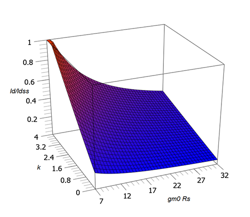
Figure \(\PageIndex{5}\): Combination Bias Surface Plot.
The graphs of Figure 10.4.13 represent three slices from this surface.
Looks cool, but...