
11.5: Noise
- Page ID
- 41339

Amplifiers, filters, and mixers in an RF front end process (e.g., amplify, filter, and mix) input noise the same way as an input signal. In addition, these modules contribute excess noise of their own. Without loss of generality, the following discussion considers noise with respect to the amplifier shown in Figure \(\PageIndex{2}\)(a), where \(v_{s}\) is the input signal. The noise signal, with source designated by \(v_{n}\), is uncorrelated and random, and described as an RMS voltage or by its noise power.
11.5.1 Noise Figure
The most important noise-related metric is the \(\text{SNR}\). Denoting the noise power input to the amplifier as \(N_{i}\), and denoting the signal power input to the amplifier as \(S_{i}\), the input signal-to-noise power ratio is \(\text{SNR}_{i} = S_{i}/N_{i}\). If the amplifier is noise free, then the input noise and signal powers are amplified by the power gain of the amplifier, \(G\). Thus the output noise power is \(N_{o} = GN_{i}\), the output signal power is \(S_{o} = GS_{i}\), and the output \(\text{SNR}\) is
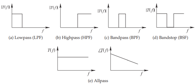
Figure \(\PageIndex{1}\): Ideal filter transfer function, \(T(f)\), responses.
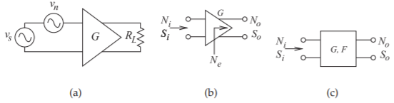
Figure \(\PageIndex{2}\): Noise and two-ports: (a) amplifier; (b) amplifier with excess noise; and (c) noisy two-port network.
\(\text{SNR}_{o}=S_{o}/N_{o}=\text{SNR}_{i}\).
In practice, an amplifier is noisy, with the addition of excess noise, Ne, indicated in Figure \(\PageIndex{2}\)(b). The excess noise originates in different components in the amplifier and is either referenced to the input or to the output of the amplifier. Most commonly it is referenced to the output so that the total output noise power is \(N_{o} = GN_{i} + N_{e}\). In the absence of a qualifier, the excess noise should be assumed to be referred to the output. \(N_{e}\) is not measured directly. Instead, the ratio of the \(\text{SNR}\) at the input to that at the output is measured and called the noise factor, \(F\):
\[\label{eq:1}F=\frac{\text{SNR}_{i}}{\text{SNR}_{o}} \]
If the circuit is noise free, then \(\text{SNR}_{o} = \text{SNR}_{i}\) and \(F = 1\). If the circuit is not noise free, then \(\text{SNR}_{o} < \text{SNR}_{i}\) and \(F > 1\). With the excess noise, referred to the output,
\[\label{eq:2}F=\frac{SNR_{i}}{\text{SNR}_{o}}=\frac{\text{SNR}_{i}}{1}\frac{1}{\text{SNR}_{o}}=\frac{S_{i}}{N_{i}}\frac{N_{o}}{S_{o}}=\frac{S_{i}}{N_{i}}\frac{GN_{i}+N_{e}}{GS_{i}}=1+\frac{N_{e}}{GN_{i}} \]
One of the conclusions that can be drawn from this is that \(F\) depends on the available noise power at the input of the circuit. As reference, the available noise power, \(N_{R}\), from a resistor at standard temperature, \(T_{0}\) (\(290\text{ K}\)), and over bandwidth, \(B\) (in \(\text{Hz}\)), is used,
\[\label{eq:3}N_{i}=N_{R}=kT_{0}B \]
where \(k (= 1.381\times 10^{−23}\text{ J/K})\) is the Boltzmann constant. If the input of an amplifier is connected to this resistor and all of the available noise power is delivered to the amplifier, then
\[\label{eq:4}F=1+\frac{N_{e}}{GN_{i}}=1+\frac{N_{e}}{GkT_{0}B} \]
When expressed in decibels, the noise figure (NF) is used:
\[\text{NF}=10\log_{10}F=\text{SNR}_{i}|_{\text{dB}}-\text{SNR}_{o}|_{\text{dB}}\nonumber \]
where the SNR is expressed in decibels. Rearranging Equation \(\eqref{eq:4}\), the output-referred excess noise power is
\[\label{eq:5}N_{e}=(F-1)GkT_{0}B \]
Also from Equation \(\eqref{eq:4}\), the output noise is
\[\label{eq:6}N_{o}=GN_{i}+N_{e}=FGN_{i} \]
That is,
\[\label{eq:7}N_{o}|_{\text{dBm}}=\text{NF}+G|_{\text{dB}}+N_{i}|_{\text{dBm}} \]
Example \(\PageIndex{1}\): Noise Figure of an Attenuator
What is the noise figure of a \(20\text{ dB}\) attenuator in a \(50\:\Omega\) system?
Solution
The appropriate circuit model to use in the analysis consists of the attenuator driven by a generator with a \(50\:\Omega\) source impedance, and the attenuator drives a \(50\:\Omega\) load. Also, the input impedance of the terminated attenuator is \(50\:\Omega\), as is the impedance looking into the output of the attenuator when it is connected to the source. The key point is that the noise coming from the source is the noise thermally generated in the \(50\:\Omega\) source impedance, and this noise is equal to the noise that is delivered to the load. So the input noise, \(N_{i}\), is equal to the output noise:
\[\label{eq:8}N_{o}=N_{i} \]
The input signal is attenuated by \(20\text{ dB} (= 100)\), so
\[\label{eq:9}S_{o}=S_{i}/100 \]
and thus the noise factor is
\[\label{eq:10}F=\frac{\text{SNR}_{i}}{\text{SNR}_{o}}=\frac{S_{i}}{N_{i}}\frac{N_{o}}{S_{o}}=\frac{S_{i}}{N_{i}}\frac{N_{i}}{S_{i}/100}=100 \]
and the noise figure is
\[\label{eq:11}\text{NF}=20\text{ dB} \]
That is, the noise figure of an attenuator (or a filter) is just the loss of the component. This is not true for amplifiers of course, as there are other sources of noise, and the output impedance of a transistor is not a thermal resistance.
11.5.2 Noise of a Cascaded System
Section 11.5.1 developed the noise factor and noise figure measures for a twoport. This can be generalized for a system. Considering the second stage of the cascade in Figure \(\PageIndex{3}\), the excess noise at the output of the second stage, due solely to the noise generated internally in the second stage, is
\[\label{eq:12}N_{2e}=(F_{2}-1)kT_{0}BG_{2} \]
Then the total noise power at the output of the two-stage cascade is
\[\begin{align}N_{2o}&=(F_{2}-1)kT_{0}BG_{2}+N_{o,1}G_{2}\nonumber \\ \label{eq:13} &=(F_{2}-1)kT_{0}BG_{2}+F_{1}kT_{0}BG_{1}G_{2}\end{align} \]
This assumes (correctly) that the excess noise added in one stage is uncorrelated to the other sources of noise. Thus noise powers can be added. Generalizing this result the total system noise factor:
\[\label{eq:14}F^{T}=F_{1}+\frac{F_{2}-1}{G_{1}}+\frac{F_{3}-1}{G_{1}G_{2}}+\frac{F_{4}-1}{G_{1}G_{2}G_{3}}+\cdots \]
This equation is known as Friis’s formula [3].
Figure \(\PageIndex{3}\): Cascaded noisy two-ports.
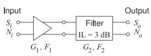
Figure \(\PageIndex{4}\): Differential amplifier followed by a differential filter.
Example \(\PageIndex{2}\): Noise Figure of Cascaded Stages
Consider the cascade of a differential amplifier and a filter shown in Figure \(\PageIndex{4}\).
- What is the midband gain of the filter in decibels? Note that IL is insertion loss.
- What is the midband noise figure of the filter?
- The amplifier has a gain \(G_{1} = 20\text{ dB}\) and a noise figure of \(2\text{ dB}\). What is the overall gain of the cascade system in the middle of the band?
- What is the noise factor of the cascade system?
- What is the noise figure of the cascade system?
Solution
- \(G_{2}=1/\text{IL}\), thus \(G_{2}=-3\text{ dB}\).
- For a passive element, \(\text{NF}_{2}=\text{IL}=3\text{ dB}\).
- \(G_{1}=20\text{ dB}\) and \(G_{2}=-3\text{ dB}\), so \(G_{\text{TOTAL}}=G_{1}|_{\text{dB}}+G_{2}|_{\text{dB}}=17\text{ dB}\).
- \(F_{1}=10^{\text{NF}_{1}/10}=10^{2/10}=1.585,\: F_{2}10^{\text{NF}_{2}/10}=10^{3/10}=1.995,\: G_{1}=10^{20/10}=100,\) and \(G_{2}=10^{-3/10}=0.5\). Using Friis's formula
\[\label{eq:15}F_{\text{TOTAL}}=F_{1}+\frac{F_{2}-1}{G_{1}}=1.585+\frac{1.995-1}{100}=1.594 \] - \(\text{NF}_{\text{TOTAL}}=10\log_{10}(\text{F}_{\text{TOTAL}})=10\log_{10}(1.594)=2.03\text{ dB}\).
Example \(\PageIndex{3}\): Noise Figure of a Two-Stage Amplifier
Consider a room-temperature (\(20^{\circ}\text{C}\)) two-stage amplifier where the first stage has a gain of \(10\text{ dB}\) and the second stage has a gain of \(20\text{ dB}\). The noise figure of the first stage is \(3\text{ dB}\) and the second stage is \(6\text{ dB}\). The amplifier has a bandwidth of \(10\text{ MHz}\).
- What is the noise power presented to the amplifier in \(10\text{ MHz}\)?
- What is the total gain of the amplifier?
- What is the total noise factor of the amplifier?
- What is the total noise figure of the amplifier?
- What is the noise power at the output of the amplifier in \(10\text{ MHz}\)?
Solution
- Noise power of a resistor at room temperature is \(−174\text{ dBm/Hz}\) (or more precisely \(−173.86\text{ dBm/Hz}\) at \(293\text{ K}\)). In \(10\text{ MHz}\) the input noise power is
\(N_{i}=-173.86\text{ dBM}+10\log (10^{7})=-173.86+70\text{ dBm}=-103.86\text{ dBm}\) - Total gain \(G^{T} = G_{1}G_{2} = 10\text{ dB} + 20\text{ dB} = 30\text{ dB} = 1000\).
- \(F_{1} = 10^{\text{NF}_{1/10}} = 10^{3/10} = 1.995,\: F_{2} = 10^{\text{NF}_{2/10}} = 10^{6/10} = 3.981\). Using Friis’s formula, the total noise figure is \(F^{T} = F_{1} +\frac{F_{2} − 1}{G_{1}} = 1.995 + \frac{3.981 − 1}{10} = 2.393\).
- The total noise figure is \(\text{NF}^{T} = 10 \log_{10}(F^{T}) = 10 \log_{10}(2.393) = 3.79\text{ dB}\).
- Output noise power in \(10\text{ MHz}\) bandwidth is \(N_{o} = F^{T}kT_{0}BG^{T} = (2.393)\cdot (1.3807\cdot 10^{−23}\cdot\text{J}\cdot\text{K}^{-1})\cdot (293\text{ K})\cdot (10^{7}\cdot s^{−1})(1000) = 9.846\cdot 10^{−11}\text{ W} = −70.07\text{ dBm}\).
Alternatively, \(N_{o}|_{\text{dBm}} = N_{i}|_{\text{dBm}} + G^{T}|_{\text{dB}} + NF^{T} = −103.86\text{ dBm} + 30\text{ dB} + 3.79\text{ dB} = −70.07\text{ dBm}\).
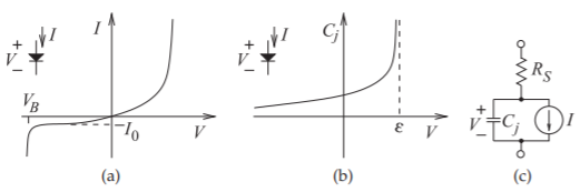
Figure \(\PageIndex{5}\): Characteristics of a pn junction diode or a Schottky diode: (a) current-voltage characteristic; (b) capacitance-voltage characteristic; and (c) diode model.