
5.4: Voltage Divider Bias
- Page ID
- 25414

Another configuration that can provide high bias stability is voltage divider bias. Instead of using a negative supply off of the emitter resistor, like two-supply emitter bias, this configuration returns the emitter resistor to ground and raises the base voltage. So as to avoid issues with a second power supply, this base voltage is derived from the collector power supply via a voltage divider. The bias template is shown in Figure \(\PageIndex{1}\).
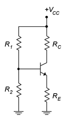
Figure \(\PageIndex{1}\): Voltage divider bias.
Let's derive the equations for the load line. First, let's consider the saturation and cutoff endpoints. For saturation, assume \(V_{CE}\) goes to 0. What resistances are left to limit the current?
\[I_{C(sat)} = \frac{V_{CC}}{R_C+R_E} \label{5.6} \]
\(V_{CE(cutoff)}\) occurs when \(I_C = 0\) and that means that there will be no potentials across \(R_C\) and \(R_E\). Therefore, \(V_{CE}\) takes on the entire available source voltage.
\[V_{CE (cutoff )} = V_{CC} \label{5.7} \]
The key to finding the Q point (and pretty much any other current or voltage in the circuit) is to find \(I_C\). To simplify the process, Thevenize the voltage divider as shown in Figure \(\PageIndex{2}\).
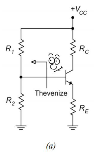
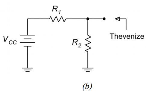
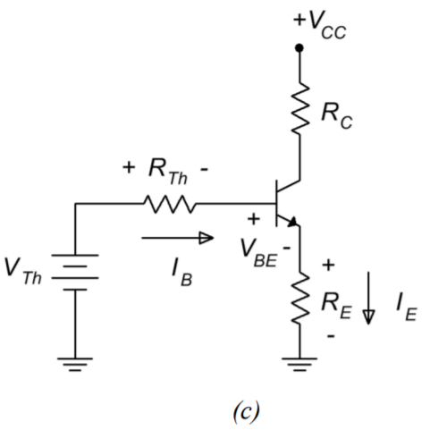
Figure \(\PageIndex{2}\): Thevenizing the voltage divider.
By inspection of Figure \(\PageIndex{2b}\),
\[V_{TH} = V_{CC} \frac{R_2}{R_1+R_2} \nonumber \]
\[R_{TH} = R_1 || R_2 = \frac{R_1 R_2}{R_1+R_2} \nonumber \]
Now we can derive an equation for the collector current by applying KVL to the base-emitter loop of Figure \(\PageIndex{2c}\):
\[V_{TH} = V_{R_{TH}} +V_{BE}+V_{R_E} \nonumber \]
\[V_{TH} = I_B R_{TH} + V_{BE} + I_E R_E \nonumber \]
Recalling that \(I_B = I_C/ \beta \) and \(I_E \approx I_C\),
\[V_{TH} = (I_C / \beta )R_{TH} + V_{BE}+I_C R_E \nonumber \]
Solving for \(I_C\) we arrive at
\[I_C = \frac{V_{TH} − V_{BE}}{R_E+R_{TH} / \beta} \label{5.8} \]
Can we find a quick approximation for \(I_C\) as well? If we assume that the voltage divider of \(R_1\) and \(R_2\) is lightly loaded, in other words, that the divider current is much, much less than the base current, finding \(I_C\) is easy. The divider voltage yields the base voltage. We then subtract the 0.7 volt drop on the base-emitter and what's left drops across \(R_E\). From there it's one short application of Ohm's law to get \(I_E\), which is approximately equal to \(I_C\). But how do we know if the divider is lightly loaded in the first place without going through the Thevenin equivalent? Looking at Equation \ref{5.8}, as long as \(R_E \gg R_{TH}/ \beta \), we can ignore the second term in the denominator, leaving us with our quick approximation. Given typical values for \( \beta \), as long as \(R_2\) is not much larger than \(R_E\), the approximation will be reasonably accurate.
Once \(I_C\) is obtained we can find the transistor's collector-emitter voltage, \(V_{CE}\),
\[V_{CE} = V_{CC} −V_{R_C} −V_{R_E} \\ V_{CE} = V_{CC} −I_C R_C −I_C R_E \\ V_{CE} = V_{CC} −I_C (R_C+R_E ) \label{5.9} \]
Time for yet another thrilling illustrative example.
Example \(\PageIndex{1}\)
Assuming \( \beta = 200\), plot the Q point (\(I_C\) and \(V_{CE}\)) on the load line for the circuit of Figure \(\PageIndex{3}\). Also determine the value of \(V_B\).
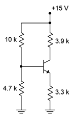
Figure \(\PageIndex{3}\): Circuit for Example \(\PageIndex{1}\).
Calculate the load line endpoints so we know the maximums.
\[I_{C(sat)} = \frac{V_{CC}}{R_C+R_E} \nonumber \]
\[I_{C(sat)} = \frac{15 V}{3.9K \Omega +3.3K \Omega} \nonumber \]
\[I_{C(sat)} = 2.08mA \nonumber \]
\[V_{CE (cutoff )} = V_{CC} \nonumber \]
\[V_{CE (cutoff )} = 15 V \nonumber \]
To obtain the Q point, first find the Thevenin values.
\[V_{TH} = V_{CC} \frac{R_2}{R_1+R_2} \nonumber \]
\[V_{TH} = 15 V \frac{4.7k\Omega}{ 10 k\Omega +4.7 k\Omega} \nonumber \]
\[V_{TH} = 4.8V \nonumber \]
\[R_{TH} = R_1 ∣∣ R_2 = \frac{R_1 R_2}{R_1+R_2} \nonumber \]
\[R_{TH} = \frac{10 k \Omega \times 4.7 k\Omega}{10 k \Omega +4.7 k\Omega} \nonumber \]
\[R_{TH} = 3.2k\Omega \nonumber \]
Using Equation \ref{5.8}:
\[I_C = \frac{V_{TH} −V_{BE}}{R_E+R_{TH} / \beta} \nonumber \]
\[I_C = \frac{4.8V −0.7V}{3.3 k\Omega +3.2 k\Omega /200} \nonumber \]
\[I_C = 1.236mA \nonumber \]
Noting the relative sizes of \(R_E\) and \(R_2\), the approximation should be fairly accurate.
\[I_C = \frac{V_{TH} −V_{BE}}{R_E} \nonumber \]
\[I_C = \frac{4.8V −0.7 V}{3.3k \Omega} \nonumber \]
\[I_C = 1.242mA \nonumber \]
To find \(V_{CE}\) we can use Equation \ref{5.9}.
\[V_{CE} = V_{CC} −I_C (R_C+R_E ) \nonumber \]
\[V_{CE} = 15V −1.236mA(3.9k \Omega +3.3 k \Omega ) \nonumber \]
\[V_{CE} = 6.1V \nonumber \]
As far as finding \(V_B\) is concerned, a decent approximation would be the value of \(V_{TH}\) because we have determined that the divider is lightly loaded. In a more general sense, we could also find the drop across \(R_E\) and then add \(V_{BE}\). The approximation yields 4.8 volts and the more accurate method yields
\[V_B = V_{BE} +I_C R_E \nonumber \]
\[V_B = 0.7 V +1.236mA\times 3.3k \Omega \nonumber \]
\[V_B = 4.78V \nonumber \]
The load line for the circuit in Example \(\PageIndex{1}\) is shown in Figure \(\PageIndex{4}\).
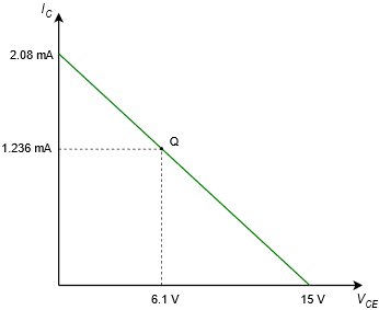
Figure \(\PageIndex{4}\): DC load line for the circuit of Figure \(\PageIndex{3}\).
Once again the proportions between voltage and current for the Q point appear to be proper when compared against the endpoints.
5.4.1: Verification of Stability
How much does the Q point move if \( \beta \) were to get cut half? Recalculating with a \( \beta \) of 100 yields \(I_C = 1.23\) mA and \(V_{CE} = 6.14\) V. This represents a shift in both current and voltage of less than 1%. This will, of course, cause a near doubling of \(I_B\) but this will be hardly noticed here as the divider current is so much larger; approximately 15V/ (10 k + 4.7 k) or 1 mA versus about 1.23 mA/100 or 12.3 \(\mu\)A.
5.4.2: PNP Voltage Divider Bias
To create the PNP version of the voltage divider bias, we replace the NPN with a PNP and then change the sign of the power supply. As mentioned with the two-supply emitter bias, these circuits are usually flipped top to bottom resulting in the flow of DC current going down the page. All of the currents and component voltages are unchanged except that their directions and polarities are reversed. The current equations and so forth remain valid. Something a little odd-looking happens with the voltage divider bias, though: we end up with ground being the most positive potential and a negative supply at the bottom of the schematic. It works, but it's an issue if we're using a traditional positive supply elsewhere in the circuit. After all, why have two supplies where one will do? It turns out that we can make a positive supply version fairly easily. All we need to do is add the magnitude of the negative source voltage to the ground and power connections. This progression is shown in Figure \(\PageIndex{5}\).
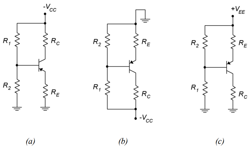
Figure \(\PageIndex{5}\): Progression of PNP voltage divider bias circuit. a. Direct conversion from NPN. b. Top-to-bottom flip. c. DC supply offset added to achieve a positive supply.
There is nothing magic about this procedure. In essence, all we've really done is renamed the reference point. All of the individual component voltages remain unchanged. For example, looking at Figure \(\PageIndex{5c}\) versus \(\PageIndex{5b}\), it is still the case that the top connection to \(R_E\) is more positive than the bottom connection to \(R_C\) by the voltage \(V_{CC}\) (although we did rename the supply to \(V_{EE}\) to be consistent with where it's connected). What has happened is that all ground-referenced (i.e., single subscript) voltages have changed. For example, \(V_B\) in Figures \(\PageIndex{5a}\) and \(\PageIndex{5b}\) is the voltage across \(R_2\). In contrast, \(V_B\) in Figure \(\PageIndex{5c}\) is the voltage across \(R_1\). That makes sense. If we move the reference then any voltage that is measured against the reference will change.
When analyzing the PNP voltage divider, we could simply parrot the collector current formula developed for the NPN, but there are other techniques. Two methods are illustrated in the following example.
Example \(\PageIndex{2}\)
Assuming \( \beta = 200\), determine the Q point (\(I_C\) and \(V_{CE}\)) for the circuit of Figure \(\PageIndex{3}\). Also determine the values of \(V_C\) and \(V_B\).
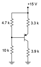
Figure \(\PageIndex{6}\): Circuit for Example \(\PageIndex{2}\).
First off, \(R_2\) (now on top) is around the same size as \(R_E\) so the approximation method should be accurate and we can assume the divider is lightly loaded.
Method One
We will focus on the base-emitter loop as usual because \(V_{BE}\) is a known potential. Our immediate goal is to find the voltage across \(R_E\) so that we can use Ohm's law to find \(I_C\). First we note that the voltage drop across \(R_2\) is equal to the combined drops across \(R_E\) and \(V_{BE}\). The drop across \(R_2\) is found via the voltage divider rule.
\[V_{R_2} = V_{EE} \frac{R_2}{R_1+R_2} \nonumber \]
\[V_{R_2} = 15 V \frac{4.7k \Omega}{ 10 k \Omega +4.7k \Omega} \nonumber \]
\[V_{R_2} = 4.8 V \nonumber \]
And
\[V_{R_E} = V_{R_2} −V_{BE} \nonumber \]
\[V_{R_E} = 4.8V−0.7V \nonumber \]
\[V_{R_E} = 4.1V \nonumber \]
Therefore
\[I_C = \frac{V_{R_E}}{R_E} \nonumber \]
\[I_C = \frac{4.1 V}{3.3 k\Omega} \nonumber \]
\[I_C = 1.24 mA \nonumber \]
Method Two
Here we will determine all voltages with respect to ground.
\[V_B = V_{EE} \frac{R_1}{R_1+R_2} \nonumber \]
\[V_B = 15 V \frac{10 k\Omega}{10 k \Omega +4.7 k\Omega} \nonumber \]
\[V_B = 10.2 V \nonumber \]
The voltage from base to emitter has a − to + polarity, meaning it is a rise of 0.7 volts. Therefore
\[V_E = V_B+V_{BE} \nonumber \]
\[V_E = 10.2V+0.7V \nonumber \]
\[V_E = 10.9V \nonumber \]
The voltage across \(R_E\) is the difference between \(V_{EE}\) and \(V_E\).
\[V_{R_E} = V_{EE}−V_E \nonumber \]
\[V_{R_E} = 15 V−10.9 V \nonumber \]
\[V_{R_E} = 4.1V \nonumber \]
This is the same value we arrived at using method one, so the collector current must be the same at 1.24 mA.
To find \(V_{CE}\) we also have options. One path is to use a slightly modified Equation \ref{5.9}.
\[V_{CE} = −(V_{EE} −I_C (R_C+R_E )) \nonumber \]
\[V_{CE} = −15V +1.24 mA (3.9 k\Omega +3.3 k\Omega ) \nonumber \]
\[V_{CE} = −6.07V \nonumber \]
The collector is negative relative to the emitter, hence the negative sign. To avoid this, we could just swap the leads and refer to \(V_{EC}\) instead.
Alternately, we could find \(V_{CE}\) by determining \(V_C\) and then subtracting \(V_E\) from it.
\[V_C = I_C R_C \nonumber \]
\[V_C = 1.24 mA\times 3.9 k\Omega \nonumber \]
\[V_C = 4.84 V \nonumber \]
\[V_{CE} = V_C−V_E \nonumber \]
\[V_{CE} = 4.84 V−10.9 V \nonumber \]
\[V_{CE} = −6.06V \nonumber \]
We see a very slight difference here due to carried rounding errors.
It is instructive to compare the results of Example \(\PageIndex{2}\) back to Example \(\PageIndex{1}\). These circuits are otherwise identical except for the fact that one is NPN and the other is PNP. We find the same results for device currents (\(I_C\)) and component voltage magnitudes (\(V_{CE}\) or the voltage across \(R_E\)); only the signs and directions are reversed. On the other hand, we find that ground referenced potentials such as \(V_B\), \(V_C\) and \(V_E\) are decidedly different between the two circuits.