
15.3: IGBT Data Sheet Interpretation
- Page ID
- 25349

A portion of the data sheet for the Fairchild/ON Semiconductor FGH50T65SQD IGBT is shown in Figure \(\PageIndex{1}\). This is a fourth generation IGBT featuring trench construction. It is rated for 650 volts and 50 amps. The device includes an antiparallel diode. This is useful for bridge applications that drive inductive loads (recall that the current through an inductor cannot change instantaneously, thus, when devices are switched on/off in a bridge, the diode serves to create a path around the IGBT for this current).

Figure \(\PageIndex{1a}\): FGH50T65SQD data sheet. Used with permission from SCILLC dba ON Semiconductor.
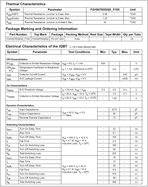
Figure \(\PageIndex{1b}\): FGH50T65SQD data sheet (cont).
The main features are the 650 volt rating for \(V_{CE}\), 100 amp continuous collector current and 268 watt dissipation at 25\(^{\circ}\)C. The current and power ratings are essentially halved at the more practical temperature of 100\(^{\circ}\)C. The threshold voltage, \(V_{GE(th)}\), is specified as 4.5 volts with a \(\pm\)1.9 volt spread. The saturation voltage typically is 1.6 volts at room temperature with 50 amps of collector current. This compares favorably to basic power BJTs. Like power MOSFETs, the input capacitance is relatively high at 3275 pF, so the same gate drive precautions must be followed. Finally, note the asymmetry in switching times. At room temperature and 12.5 amps of collector current, the turn-on delay plus rise time is specified as approximately 31 nanoseconds while the turn-off delay and fall time is nearly 110 nanoseconds. This relative slowing of the off-state transition is typical of IGBTs. Further, as both current and temperature increase (Figure \(\PageIndex{1c}\)), these times increase by a few percent. By comparison, the FDMS86180 power E-MOSFET examined in Chapter 12 exhibited symmetrical values in the mid-30 nanosecond region at a drain current of 67 amps.
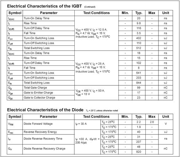
Figure \(\PageIndex{1c}\): FGH50T65SQD data sheet (cont).
Finally, consider the graphical data presented in Figure \(\PageIndex{1d}\).
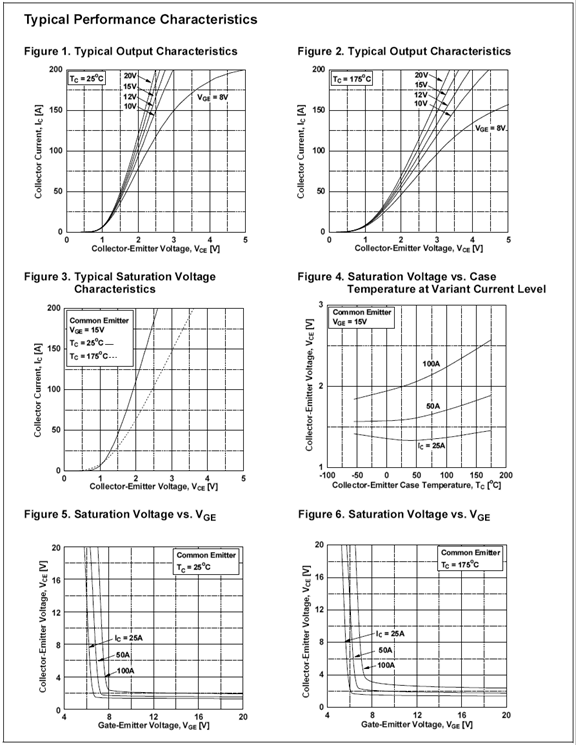
Figure \(\PageIndex{1d}\): FGH50T65SQD data sheet (cont).
The top two graphs show the collector curves in the low voltage region. Compare these with Figure 15.2.3. Similarly, the middle-left graph shows the current-voltage characteristic with temperature variation. This reflects Figure 15.2.4. Finally, the bottom two graphs show the collector-emitter saturation voltage with respect to gateemitter drive voltage for three different collector currents. Note that for the highest current at room temperature, saturation voltage is around 2 volts for a gate drive of at least 8 volts. This rises to about 3 volts at 175\(^{\circ}\)C.
Computer Simulation
To highlight the performance of the IGBT, a simple series load switch is simulated. The circuit is shown in Figure \(\PageIndex{2}\).
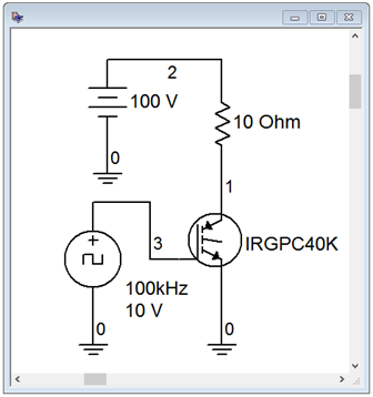
Figure \(\PageIndex{2}\): IGBT simulation schematic.
A 10 ohm load is switched from a 100 volt DC power supply via an International Rectifier IRGPC40K IGBT. The gate is driven from a 10 volt peak square wave running at 100 kHz.
Ideally, if the IGBT produced no losses, the full 100 volt source would drop across the load, producing 10 amp current pulses. According to the device data sheet, collector-emitter saturation voltage typically is 2.1 volts (3.2 volts maximum) with a 25 amp collector current. The total turn-on/rise time and turn-off/fall time values are 62 nanoseconds and 290 nanoseconds typically, at 25 amps and room temperature.
A transient analysis is run, with the results shown in Figure \(\PageIndex{3}\).
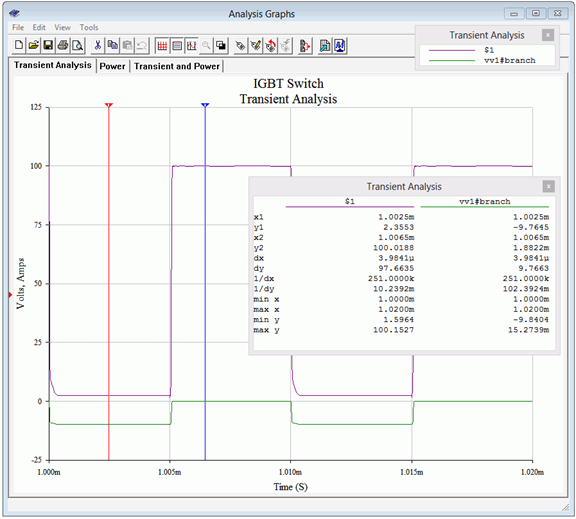
Figure \(\PageIndex{3}\): Transient analysis of simple IGBT switch.
The drain voltage (node 1) is shown as the purple trace and the drain current is shown in green (reversed in polarity to see it more clearly). The two cursors (red is #1, blue is #2) show the various levels. As expected, the drain voltage peaks at 100 volts in the off-state, at which time the current is nil. During the on-state, the drain voltage drops to about 2.36 volts, very close to the data sheet's typical saturation potential. This small drop reduces the voltage across the load to about 97.64 volts. This is verified by cursor #1 showing a current of 9.765 amps. Also, although it is not possible to determine the edge timings with great precision from this plot, the asymmetry between rise and fall is apparent, and the edges are generally consistent with the numeric values from the data sheet.
Figure \(\PageIndex{4}\): shows the result of multiplying the current and voltage waveforms. This new waveform represents the power dissipation of the IGBT.
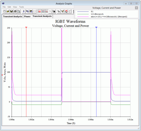
Figure \(\PageIndex{4}\): Power waveform of simple IGBT switch.
The power trace is shown in fuchsia, or magenta, or screaming purple-pink, or whatever-you-want-to-call-it. The edge spikes dominate but the on-state power is apparent as well. Remember, during the on-state, the load is dissipating close to 1000 watts. The cursor output window is shown separately in Figure \(\PageIndex{5}\). The on-state power dissipation is approximately 23 watts which represents less than 2.5 percent of the load power. In contrast, the edge spikes are maxing out at around 250 watts. Of course, the time duration is very short, being only a few percent of the cycle period, but it cannot be ignored.
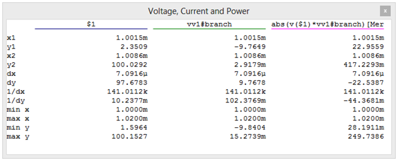
Figure \(\PageIndex{5}\): Numeric values at waveform cursors for the IGBT switch.