
15.2: IGBT Internals
- Page ID
- 25348

The IGBT is a multi-layer device. The cutaway shown in Figure \(\PageIndex{1}\) uses an Nchannel, although P-channel is possible. This device has many features in common with the power E-MOSFET discussed in Chapter 12.
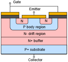
Figure \(\PageIndex{1}\): Cutaway view of IGBT.
To begin, note the labeling of the three terminals: gate, emitter and collector. The gate is isolated just as it is in MOSFETs. When a positive gate-emitter potential is applied, an N-type inversion layer will develop in the the P body region, allowing current to flow. The middle N region is split into two sections, the main N− drift region and the N+ buffer layer (the +/− signs indicate heavy and light doping, respectively). The device shown is the punch through (PT) variety. The non-punch through (NPT) omits the buffer layer. The functional differences between the two are that splitting the N material to include the buffer layer improves speed and lowers on-state voltage. Consequently, the PT version exhibits lower switching and conduction losses.
The upper three layers of Figure \(\PageIndex{1}\) form an E-MOSFET while the lower section (P body, N drift/buffer and P substrate) form a PNP transistor. Thus, we can make a simplified model of the IGBT using these other devices, as shown in Figure 12.2.2.
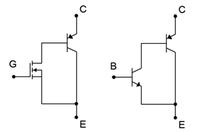
Figure \(\PageIndex{2}\): Simple model of an IGBT (left) compared to a Sziklai pair (right).
This simplified model is reminiscent of the NPN version of the Sziklai pair examined in Chapter 9. The input device has been replaced by an E-MOSFET. Therefore we expect the very small gate current and relatively simple drive requirements of the EMOSFET with the power handling of a BJT.
The operational device curves are, unsurprisingly, also reminiscent of these two components. A set of collector curves is presented in Figure \(\PageIndex{3}\) using representative values for voltage and current.
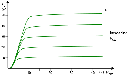
Figure \(\PageIndex{3}\): IGBT collector curve family.
This set of curves appears as a cross between the collector curve family seen in Chapter 4 and the drain curve family seen in Chapter 10, with one slight twist: the entire set of curves is displaced positively from the origin by about one volt. As with any E-MOSFET, channel current does not begin to flow until the gate threshold voltage is reached, here referred to as \(V_{GE(th)}\). Increasing values of \(V_{GE}\) cause increased conduction and current flow. Finally, note that the curves do not begin to “flatten” until \(V_{CE}\) has reached several volts, unlike the saturation voltage of a single BJT which might be only tenths of a volt.
The forward current-voltage characteristic curve reflects the E-MOSFET portion of the model. This is shown in Figure \(\PageIndex{4}\).
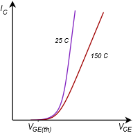
Figure \(\PageIndex{4}\): IGBT characteristic curve and variation with temperature.
Two traces are plotted for two different temperatures. The curves are essentially the same as the characteristic curve of the E-MOSFET, as seen in the introductory MOSFET chapter, Figure 12.4.3 (here the current axis has been expanded, making the traces appear steeper, in order to more clearly show the variation with temperature). Conduction begins at the threshold voltage, \(V_{GE(th)}\), and then rises rapidly, following a square law trajectory. Once a sufficient current level is reached, the curve can be approximated as a straight line.
Of particular interest here is how the curve varies with temperature. As temperature increases (red trace), the slope decreases. Recalling that the slope of the current-voltage characteristic curve is the device transconductance, this means that the transconductance decreases with temperature. In other words, the IGBT exhibits a negative temperature coefficient of transconductance, just like power E-MOSFETs, and thus are also less inclined to suffer from current hogging and thermal runaway problems than BJTs.
Unfortunately, there isn't a single, standardized schematic symbol for the IGBT. Two versions are shown in Figure \(\PageIndex{5}\).
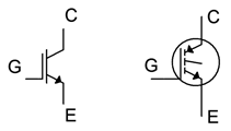
Figure \(\PageIndex{5}\): IGBT schematic symbols.
Both symbols attempt to reflect the dual E-MOSFET/BJT character of the device. The symbol on the left appears to have wider use currently, although there is also a third variation based on it where the gate connection is drawn toward the center rather than closer to the emitter.