2.1: Intro to Bipolar Resistors
- Page ID
- 88527
\( \newcommand{\vecs}[1]{\overset { \scriptstyle \rightharpoonup} {\mathbf{#1}} } \)
\( \newcommand{\vecd}[1]{\overset{-\!-\!\rightharpoonup}{\vphantom{a}\smash {#1}}} \)
\( \newcommand{\id}{\mathrm{id}}\) \( \newcommand{\Span}{\mathrm{span}}\)
( \newcommand{\kernel}{\mathrm{null}\,}\) \( \newcommand{\range}{\mathrm{range}\,}\)
\( \newcommand{\RealPart}{\mathrm{Re}}\) \( \newcommand{\ImaginaryPart}{\mathrm{Im}}\)
\( \newcommand{\Argument}{\mathrm{Arg}}\) \( \newcommand{\norm}[1]{\| #1 \|}\)
\( \newcommand{\inner}[2]{\langle #1, #2 \rangle}\)
\( \newcommand{\Span}{\mathrm{span}}\)
\( \newcommand{\id}{\mathrm{id}}\)
\( \newcommand{\Span}{\mathrm{span}}\)
\( \newcommand{\kernel}{\mathrm{null}\,}\)
\( \newcommand{\range}{\mathrm{range}\,}\)
\( \newcommand{\RealPart}{\mathrm{Re}}\)
\( \newcommand{\ImaginaryPart}{\mathrm{Im}}\)
\( \newcommand{\Argument}{\mathrm{Arg}}\)
\( \newcommand{\norm}[1]{\| #1 \|}\)
\( \newcommand{\inner}[2]{\langle #1, #2 \rangle}\)
\( \newcommand{\Span}{\mathrm{span}}\) \( \newcommand{\AA}{\unicode[.8,0]{x212B}}\)
\( \newcommand{\vectorA}[1]{\vec{#1}} % arrow\)
\( \newcommand{\vectorAt}[1]{\vec{\text{#1}}} % arrow\)
\( \newcommand{\vectorB}[1]{\overset { \scriptstyle \rightharpoonup} {\mathbf{#1}} } \)
\( \newcommand{\vectorC}[1]{\textbf{#1}} \)
\( \newcommand{\vectorD}[1]{\overrightarrow{#1}} \)
\( \newcommand{\vectorDt}[1]{\overrightarrow{\text{#1}}} \)
\( \newcommand{\vectE}[1]{\overset{-\!-\!\rightharpoonup}{\vphantom{a}\smash{\mathbf {#1}}}} \)
\( \newcommand{\vecs}[1]{\overset { \scriptstyle \rightharpoonup} {\mathbf{#1}} } \)
\( \newcommand{\vecd}[1]{\overset{-\!-\!\rightharpoonup}{\vphantom{a}\smash {#1}}} \)
\(\newcommand{\avec}{\mathbf a}\) \(\newcommand{\bvec}{\mathbf b}\) \(\newcommand{\cvec}{\mathbf c}\) \(\newcommand{\dvec}{\mathbf d}\) \(\newcommand{\dtil}{\widetilde{\mathbf d}}\) \(\newcommand{\evec}{\mathbf e}\) \(\newcommand{\fvec}{\mathbf f}\) \(\newcommand{\nvec}{\mathbf n}\) \(\newcommand{\pvec}{\mathbf p}\) \(\newcommand{\qvec}{\mathbf q}\) \(\newcommand{\svec}{\mathbf s}\) \(\newcommand{\tvec}{\mathbf t}\) \(\newcommand{\uvec}{\mathbf u}\) \(\newcommand{\vvec}{\mathbf v}\) \(\newcommand{\wvec}{\mathbf w}\) \(\newcommand{\xvec}{\mathbf x}\) \(\newcommand{\yvec}{\mathbf y}\) \(\newcommand{\zvec}{\mathbf z}\) \(\newcommand{\rvec}{\mathbf r}\) \(\newcommand{\mvec}{\mathbf m}\) \(\newcommand{\zerovec}{\mathbf 0}\) \(\newcommand{\onevec}{\mathbf 1}\) \(\newcommand{\real}{\mathbb R}\) \(\newcommand{\twovec}[2]{\left[\begin{array}{r}#1 \\ #2 \end{array}\right]}\) \(\newcommand{\ctwovec}[2]{\left[\begin{array}{c}#1 \\ #2 \end{array}\right]}\) \(\newcommand{\threevec}[3]{\left[\begin{array}{r}#1 \\ #2 \\ #3 \end{array}\right]}\) \(\newcommand{\cthreevec}[3]{\left[\begin{array}{c}#1 \\ #2 \\ #3 \end{array}\right]}\) \(\newcommand{\fourvec}[4]{\left[\begin{array}{r}#1 \\ #2 \\ #3 \\ #4 \end{array}\right]}\) \(\newcommand{\cfourvec}[4]{\left[\begin{array}{c}#1 \\ #2 \\ #3 \\ #4 \end{array}\right]}\) \(\newcommand{\fivevec}[5]{\left[\begin{array}{r}#1 \\ #2 \\ #3 \\ #4 \\ #5 \\ \end{array}\right]}\) \(\newcommand{\cfivevec}[5]{\left[\begin{array}{c}#1 \\ #2 \\ #3 \\ #4 \\ #5 \\ \end{array}\right]}\) \(\newcommand{\mattwo}[4]{\left[\begin{array}{rr}#1 \amp #2 \\ #3 \amp #4 \\ \end{array}\right]}\) \(\newcommand{\laspan}[1]{\text{Span}\{#1\}}\) \(\newcommand{\bcal}{\cal B}\) \(\newcommand{\ccal}{\cal C}\) \(\newcommand{\scal}{\cal S}\) \(\newcommand{\wcal}{\cal W}\) \(\newcommand{\ecal}{\cal E}\) \(\newcommand{\coords}[2]{\left\{#1\right\}_{#2}}\) \(\newcommand{\gray}[1]{\color{gray}{#1}}\) \(\newcommand{\lgray}[1]{\color{lightgray}{#1}}\) \(\newcommand{\rank}{\operatorname{rank}}\) \(\newcommand{\row}{\text{Row}}\) \(\newcommand{\col}{\text{Col}}\) \(\renewcommand{\row}{\text{Row}}\) \(\newcommand{\nul}{\text{Nul}}\) \(\newcommand{\var}{\text{Var}}\) \(\newcommand{\corr}{\text{corr}}\) \(\newcommand{\len}[1]{\left|#1\right|}\) \(\newcommand{\bbar}{\overline{\bvec}}\) \(\newcommand{\bhat}{\widehat{\bvec}}\) \(\newcommand{\bperp}{\bvec^\perp}\) \(\newcommand{\xhat}{\widehat{\xvec}}\) \(\newcommand{\vhat}{\widehat{\vvec}}\) \(\newcommand{\uhat}{\widehat{\uvec}}\) \(\newcommand{\what}{\widehat{\wvec}}\) \(\newcommand{\Sighat}{\widehat{\Sigma}}\) \(\newcommand{\lt}{<}\) \(\newcommand{\gt}{>}\) \(\newcommand{\amp}{&}\) \(\definecolor{fillinmathshade}{gray}{0.9}\)Let's leave the world of two terminal devices (which are all called diodes by the way; diode just means two-terminals) and venture into the much more interesting world of three terminals. The first device we will look at is called the bipolar transistor. Consider the structure shown in Figure \(\PageIndex{1}\):

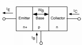
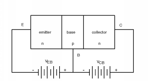
The device consists of three layers of silicon: a heavily doped n-type layer called the emitter, a moderately doped p-type layer called the base, and a third, more lightly doped layer called the collector. In a biasing (applied DC potential) configuration called forward active biasing, the emitter-base junction is forward biased, and the base-collector junction is reverse biased. Figure \(\PageIndex{2}\) shows the biasing conventions we will use. Both bias voltages are referenced to the base terminal. Since the base-emitter junction is forward biased, and since the base is made of p-type material \(V_{\text{EB}}\) must be negative. On the other hand, in order to reverse bias the base-collector junction, \(V_{\text{CB}}\) will be a positive voltage.

Now, let's draw the band-diagram for this device. At first this might seem hard to do, but we know what forward and reverse biased band diagrams look like, so we'll just stick one of each together. We show this in Figure \(\PageIndex{3}\). Figure \(\PageIndex{3}\) is a very busy figure, but it is also very important, because it shows all of the important features in the operation the transistor. Since the base-emitter junction is forward biased, electrons will go from the (n-type) emitter into the base. Likewise, some holes from the base will be injected into the emitter.

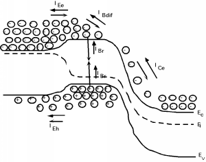
In Figure \(\PageIndex{3}\), we have two different kinds of arrows. The open arrows which are attached to the carriers, show us which way the carrier is moving. The solid arrows which are labeled with some kind of subscripted \(I\) represent current flow. We need to do this because for holes, motion and current flow are in the same direction, while for electrons, carrier motion and current flow are in opposite directions.
Just as we saw in the last chapter, the electrons which are injected into the base diffuse away from the emitter-base junction towards the (reverse biased) base-collector junction. As they move through the base, some of the electrons encounter holes and recombine with them. Those electrons which do get to the base-collector junction run into a large electric field which sweeps them out of the base and into the collector. (They "fall" down the large potential drop at the junction.)
These effects are all seen in Figure \(\PageIndex{3}\), with arrows representing the various currents which are associated with each of the carriers fluxes. \(I_{\text{Ee}}\) represents the current associated with the electron injection into the base. (It points in the opposite direction from the motion of the electrons, since electrons have a negative charge.) \(I_{\text{Eh}}\) represents the current associated with holes injection into the emitter from the base. \(I_{\text{Br}}\) represents recombination current in the base, while \(I_{\text{Ce}}\) represents the electron current going into the collector. It should be easy for you to see that:
\[I_{E} = I_{\text{Ee}} + I_{\text{Eh}} \nonumber \] \[I_{B} = I_{\text{Eh}} + I_{\text{Br}} \nonumber \] \[I_{C} = I_{\text{Ce}} \nonumber \]
In a "good" transistor, almost all of the current across the base-emitter junction consists of electrons being injected into the base. The transistor engineer works hard to design the device so that very little emitter current is made up of holes coming from the base into the emitter. The transistor is also designed so that almost all of those electrons which are injected into the base make it across to the base-collector reverse-biased junction. Some recombination is unavoidable, but things are arranged so as to minimize this effect.