4.7: Integrated Circuit Well and Gate Creation
- Page ID
- 88551

We then remove the remaining resist, and perform an activation/anneal/diffusion step, also sometimes called the "drive-in". The purpose of this step is twofold. We want to make the n-tank deep enough so that we can use it for our p-channel MOS, and we want to build up an implant barrier so that we can implant into the p-substrate region only. We introduce oxygen into the reactor during the activation, so that we grow a thicker oxide over the region where we implanted the phosphorus. The nitride layer over the p-substrate on the LHS protects that area from any oxide growth. We then end up with the structure shown in Figure \(\PageIndex{1}\).
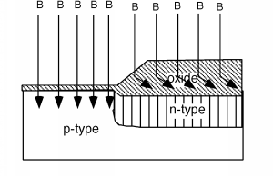
Now we strip the remaining nitride. Since the only way we can convert from p to n is to add a donor concentration which is greater than the background acceptor concentration, we had to keep the doping in the substrate fairly light in order to be able to make the n-tank. The lightly doped p-substrate would have too low a threshold voltage for good n-MOS transistor operation, so we will do a \(V_{T}\) adjust implant through the thin oxide on the left hand side, with the thick oxide on the right side blocking the boron from getting into the n-tank. This is shown in Figure \(\PageIndex{2}\), where boron is implanted into the p-type substrate on the left side, but is blocked by the thick oxide in the region over the n-well.
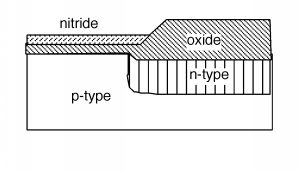
Next, we strip off all the oxide and grow a new thin layer of oxide, and then a layer of nitride (Figure \(\PageIndex{3}\)). The oxide layer is grown only because it is bad to grow \(\mathrm{Si}_{3} \mathrm{N}_{4}\) directly on top of silicon, as the different coefficients of thermal expansion between the two materials causes damage to the silicon crystal structure. Also, it turns out to be nearly impossible to remove nitride if it is deposited directly on to silicon.
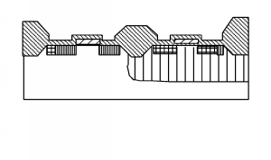
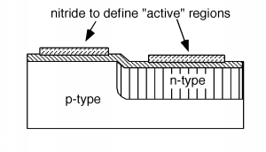
The nitride is patterned (covered with photoresist, exposed, developed, etched, and cleaned of photoresist) to make two areas which are called "active" (Figure \(\PageIndex{4}\)). (This is where we will build our transistors.) The wafer is then subjected to a high-pressure oxidation step which grows a thick oxide wherever the nitride was removed. The nitride is a good barrier for oxygen, so essentially no oxide grows underneath it. The thick oxide is used to isolate individual transistors, and also to make for an insulating layer over which conducting patterns can be run. The thick oxide is called field oxide (or FOX for short), as shown in Figure \(\PageIndex{5}\).
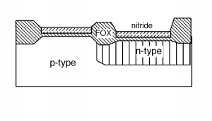
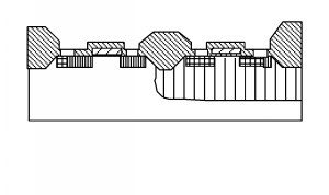
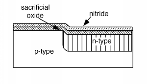
Then, the nitride and some of the oxide are etched off. The oxide is etched enough so that all of the oxide under the nitride regions is removed, which will take a little off the field oxide as well. This is because we now want to grow the gate oxide, which must be very clean and pure (Figure \(\PageIndex{6}\). The oxide under the nitride is sometimes called sacrificial oxide, because it is sacrificed in the name of ultra performance.
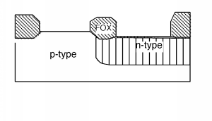 Figure \(\PageIndex{6}\): Getting ready to grow gate oxide
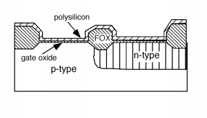
Then the gate oxide is grown, and immediately thereafter, the whole wafer is covered with polysilicon (Figure \(\PageIndex{7}\)).
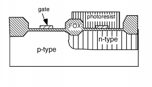
The polysilicon is then patterned to form the two regions which will be our gates. The wafer is covered once again with photoresist. The resist is removed over the region that will be the n-channel device, but is left covering the p-channel device. A little area near the edge of the n-tank is also uncovered (Figure \(\PageIndex{8}\)). This will allow us to add some additional phosphorus into the n-well, so that we can make a contact there, so that the n-well can be connected to \(V_{\text{dd}}\).
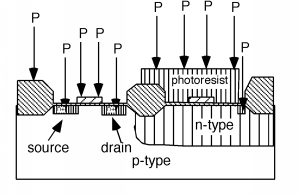
Back into the implanter we go, this time exposing the wafer to phosphorus. The poly gate, the FOX and the photoresist all block phosphorus from getting into the wafer, so we make two n-type regions in the p-type substrate, and we have made our n-channel MOS source/drain regions. We also add phosphorous to the \(V_{\text{dd}}\) contact region in the n-well so as the make sure we get good contact performance there (Figure \(\PageIndex{9}\)).
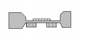
Note that the formation of the source and drain were performed with a self-aligning technology. This means that we used the gate structure itself to define where the two inside edges of the source and drain would be for the MOSFET. If we had made the source/drain regions before we defined the gate, and then tried to line the gate up right over the space between them, we might have gotten something that looks like what is shown in Figure \(\PageIndex{10}\).
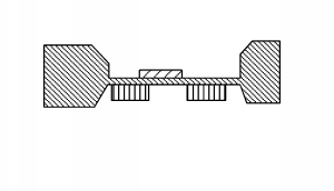
What's going to be the problem with this transistor? Obviously, if the gate does not extend all the way to both the source and the drain, then the channel will not either, and the transistor will never turn on! We could try making the gate wider, to ensure that it will overlap both active areas, even if it is slightly misaligned, but then you get a lot of extraneous fringing capacitance which will significantly slow down the speed of operation of the transistor (Figure \(\PageIndex{11}\)). This is bad! The development of the self-aligned gate technique was one of the big breakthroughs which has propelled us into the VLSI and ULSI era.
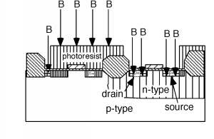
We pull the wafer out of the implanter, and strip off the photoresist. This is sometimes difficult, because the act of ion implantation can "bake" the photoresist into a very tough film. Sometimes an rf discharge in an \(\mathrm{O}_{2}\) atmosphere is used to "ash" the photoresist, and literally burn it off the wafer! We now apply some more PR, and this time pattern to have the moat area, and a substrate contact exposed, for a boron p+ implant. This is shown in Figure \(\PageIndex{12}\).
We are almost done. The next thing we do is remove all the photoresist, and grow one more layer of oxide, which covers everything, as shown in Figure \(\PageIndex{13}\). We put photoresist over the whole wafer again, and pattern for contact holes to go through the oxide. We will put contacts for the two drains, and for each of the sources, make sure that the holes are big enough to also allow us to connect the source contact to either the p-substrate or the n-moat as is appropriate (Figure \(\PageIndex{14}\)).