
11.7: Band-Pass Filter Realizations
- Page ID
- 26748

\( \newcommand{\vecs}[1]{\overset { \scriptstyle \rightharpoonup} {\mathbf{#1}} } \)
\( \newcommand{\vecd}[1]{\overset{-\!-\!\rightharpoonup}{\vphantom{a}\smash {#1}}} \)
\( \newcommand{\dsum}{\displaystyle\sum\limits} \)
\( \newcommand{\dint}{\displaystyle\int\limits} \)
\( \newcommand{\dlim}{\displaystyle\lim\limits} \)
\( \newcommand{\id}{\mathrm{id}}\) \( \newcommand{\Span}{\mathrm{span}}\)
( \newcommand{\kernel}{\mathrm{null}\,}\) \( \newcommand{\range}{\mathrm{range}\,}\)
\( \newcommand{\RealPart}{\mathrm{Re}}\) \( \newcommand{\ImaginaryPart}{\mathrm{Im}}\)
\( \newcommand{\Argument}{\mathrm{Arg}}\) \( \newcommand{\norm}[1]{\| #1 \|}\)
\( \newcommand{\inner}[2]{\langle #1, #2 \rangle}\)
\( \newcommand{\Span}{\mathrm{span}}\)
\( \newcommand{\id}{\mathrm{id}}\)
\( \newcommand{\Span}{\mathrm{span}}\)
\( \newcommand{\kernel}{\mathrm{null}\,}\)
\( \newcommand{\range}{\mathrm{range}\,}\)
\( \newcommand{\RealPart}{\mathrm{Re}}\)
\( \newcommand{\ImaginaryPart}{\mathrm{Im}}\)
\( \newcommand{\Argument}{\mathrm{Arg}}\)
\( \newcommand{\norm}[1]{\| #1 \|}\)
\( \newcommand{\inner}[2]{\langle #1, #2 \rangle}\)
\( \newcommand{\Span}{\mathrm{span}}\) \( \newcommand{\AA}{\unicode[.8,0]{x212B}}\)
\( \newcommand{\vectorA}[1]{\vec{#1}} % arrow\)
\( \newcommand{\vectorAt}[1]{\vec{\text{#1}}} % arrow\)
\( \newcommand{\vectorB}[1]{\overset { \scriptstyle \rightharpoonup} {\mathbf{#1}} } \)
\( \newcommand{\vectorC}[1]{\textbf{#1}} \)
\( \newcommand{\vectorD}[1]{\overrightarrow{#1}} \)
\( \newcommand{\vectorDt}[1]{\overrightarrow{\text{#1}}} \)
\( \newcommand{\vectE}[1]{\overset{-\!-\!\rightharpoonup}{\vphantom{a}\smash{\mathbf {#1}}}} \)
\( \newcommand{\vecs}[1]{\overset { \scriptstyle \rightharpoonup} {\mathbf{#1}} } \)
\(\newcommand{\longvect}{\overrightarrow}\)
\( \newcommand{\vecd}[1]{\overset{-\!-\!\rightharpoonup}{\vphantom{a}\smash {#1}}} \)
\(\newcommand{\avec}{\mathbf a}\) \(\newcommand{\bvec}{\mathbf b}\) \(\newcommand{\cvec}{\mathbf c}\) \(\newcommand{\dvec}{\mathbf d}\) \(\newcommand{\dtil}{\widetilde{\mathbf d}}\) \(\newcommand{\evec}{\mathbf e}\) \(\newcommand{\fvec}{\mathbf f}\) \(\newcommand{\nvec}{\mathbf n}\) \(\newcommand{\pvec}{\mathbf p}\) \(\newcommand{\qvec}{\mathbf q}\) \(\newcommand{\svec}{\mathbf s}\) \(\newcommand{\tvec}{\mathbf t}\) \(\newcommand{\uvec}{\mathbf u}\) \(\newcommand{\vvec}{\mathbf v}\) \(\newcommand{\wvec}{\mathbf w}\) \(\newcommand{\xvec}{\mathbf x}\) \(\newcommand{\yvec}{\mathbf y}\) \(\newcommand{\zvec}{\mathbf z}\) \(\newcommand{\rvec}{\mathbf r}\) \(\newcommand{\mvec}{\mathbf m}\) \(\newcommand{\zerovec}{\mathbf 0}\) \(\newcommand{\onevec}{\mathbf 1}\) \(\newcommand{\real}{\mathbb R}\) \(\newcommand{\twovec}[2]{\left[\begin{array}{r}#1 \\ #2 \end{array}\right]}\) \(\newcommand{\ctwovec}[2]{\left[\begin{array}{c}#1 \\ #2 \end{array}\right]}\) \(\newcommand{\threevec}[3]{\left[\begin{array}{r}#1 \\ #2 \\ #3 \end{array}\right]}\) \(\newcommand{\cthreevec}[3]{\left[\begin{array}{c}#1 \\ #2 \\ #3 \end{array}\right]}\) \(\newcommand{\fourvec}[4]{\left[\begin{array}{r}#1 \\ #2 \\ #3 \\ #4 \end{array}\right]}\) \(\newcommand{\cfourvec}[4]{\left[\begin{array}{c}#1 \\ #2 \\ #3 \\ #4 \end{array}\right]}\) \(\newcommand{\fivevec}[5]{\left[\begin{array}{r}#1 \\ #2 \\ #3 \\ #4 \\ #5 \\ \end{array}\right]}\) \(\newcommand{\cfivevec}[5]{\left[\begin{array}{c}#1 \\ #2 \\ #3 \\ #4 \\ #5 \\ \end{array}\right]}\) \(\newcommand{\mattwo}[4]{\left[\begin{array}{rr}#1 \amp #2 \\ #3 \amp #4 \\ \end{array}\right]}\) \(\newcommand{\laspan}[1]{\text{Span}\{#1\}}\) \(\newcommand{\bcal}{\cal B}\) \(\newcommand{\ccal}{\cal C}\) \(\newcommand{\scal}{\cal S}\) \(\newcommand{\wcal}{\cal W}\) \(\newcommand{\ecal}{\cal E}\) \(\newcommand{\coords}[2]{\left\{#1\right\}_{#2}}\) \(\newcommand{\gray}[1]{\color{gray}{#1}}\) \(\newcommand{\lgray}[1]{\color{lightgray}{#1}}\) \(\newcommand{\rank}{\operatorname{rank}}\) \(\newcommand{\row}{\text{Row}}\) \(\newcommand{\col}{\text{Col}}\) \(\renewcommand{\row}{\text{Row}}\) \(\newcommand{\nul}{\text{Nul}}\) \(\newcommand{\var}{\text{Var}}\) \(\newcommand{\corr}{\text{corr}}\) \(\newcommand{\len}[1]{\left|#1\right|}\) \(\newcommand{\bbar}{\overline{\bvec}}\) \(\newcommand{\bhat}{\widehat{\bvec}}\) \(\newcommand{\bperp}{\bvec^\perp}\) \(\newcommand{\xhat}{\widehat{\xvec}}\) \(\newcommand{\vhat}{\widehat{\vvec}}\) \(\newcommand{\uhat}{\widehat{\uvec}}\) \(\newcommand{\what}{\widehat{\wvec}}\) \(\newcommand{\Sighat}{\widehat{\Sigma}}\) \(\newcommand{\lt}{<}\) \(\newcommand{\gt}{>}\) \(\newcommand{\amp}{&}\) \(\definecolor{fillinmathshade}{gray}{0.9}\)There are many ways to form a band-pass filter. Before we introduce a few of the possibilities, we must define a number of important parameters. As in the case of the high- and low-pass filters, the concept of damping is important. For historical reasons, band-pass filters are normally specified with the parameter \(Q\), the quality factor, which is the reciprocal of the damping factor. Comparable to the break frequency is the center, or peak, frequency of the filter. This is the point of maximum gain. In RLC circuits, it is usually referred to as the resonance frequency. The symbol for center frequency is \(f_o\). Because a band-pass filter produces attenuation on either side of the center frequency, there are two “3 dB down” frequencies. The lower frequency is normally given the name \(f_1\), and the upper is given \(f_2\). The difference between \(f_2\) and \(f_1\) is called the bandwidth of the filter and is abbreviated as \(BW\). The ratio of center frequency to bandwidth is equal to the filter's \(Q\).
\[BW = f_2 − f_1 \label{11.15} \]
\[Q = \frac{f_o}{BW} \label{11.16} \]
It is important to note that the center frequency is not equal to the arithmetic average of \(f_1\) and \(f_2\). Instead, it is equal to the geometric average of \(f_1\) and \(f_2\).
\[f_o = \sqrt{f_1 f_2} \label{11.17} \]
These parameters are shown graphically in Figure \(\PageIndex{1}\). If a filter requires a fairly low \(Q\), say unity or less, the filter is best realized as a cascade of separate low- and high-pass filters. For higher \(Q\)s, we will examine two possible realizations. Multiple-feedback filters will be used for \(Q\) s up to about 10. For \(Q\) s above 10, the state-variable filter is presented.
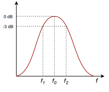
Figure \(\PageIndex{1}\): Band-pass response.
11.7.1: Multiple-Feedback Filters
The basic multiple-feedback filter is a second-order type. It contains two reactive elements as shown in Figure \(\PageIndex{2}\). One pair of elements creates the low-pass response \((R_1C_1)\), and the other pair creates the high-pass response \((R_2C_2)\). Because of this, the ultimate attenuation slopes are \(\pm 6\) dB.
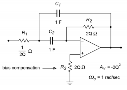
Figure \(\PageIndex{2}\): Multiple feedback band-pass filter.
As with the VCVS high- and low-pass designs, the circuit of Figure \(\PageIndex{2}\) is normalized to a 1 radian per second center frequency. Extrapolation to new center frequencies is performed in the same manner as shown earlier. The peak gain for this circuit is
\[A_v = −2Q^2 \label{11.18} \]
You can see from Equation \ref{11.18} that higher \(Q\) s will produce higher gains. For a \(Q\) of 10, the voltage gain will be 200. For this circuit to function properly, the open-loop gain of the op amp used must be greater than 200 at the chosen center frequency. Usually, a safety factor of 10 is included in order to keep stability high and distortion low. By combining these factors, we may determine the minimum acceptable \(f_{unity}\) for the op amp.
\[f_{unity} \geq 10 f_o A_v \label{11.19a} \]
or more directly,
\[f_{unity} \geq 20 f_o Q^2 \label{11.19b} \]
For a \(Q\) of 10 and a center frequency of 2 kHz, the op amp will need an \(f_{unity}\) of at least 4 MHz. It is not possible to use this type of filter for high-frequency, high-\(Q\) work, as standard op amps soon “run out of steam”. This difficulty aside, the high gains produced by even moderate values for \(Q\) may well be impractical. For many applications, a unity gain version would be preferred. This is not particularly difficult to achieve. All that we need to do is attenuate the input signal by a factor equal to the voltage gain of the filter. Because the gain magnitude of the filter is \(2Q^2\), the attenuation should be
\[Attenuation = \frac{1}{2Q^2} \label{11.20} \]
Although it is possible to place a pair of resistors in front of the filter to create a voltage divider, there is a more efficient way. We can split \(R_1\) into two components, as shown in Figure \(\PageIndex{3}\). As long as the Thevenin equivalent of \(R_{1a}\) and \(R_{1b}\) as seen from the op amp equals the value of \(R_1\), the tuning frequency of the filter will not be changed. Also required is that the voltage divider ratio produced by \(R_{1a}\) and \(R_{1b}\) satisfies Equation \ref{11.20}.
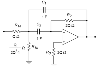
Figure \(\PageIndex{3}\): Multiple feedback filter with unity-gain variation.
First, let's determine the ratio of the two resistors. We can start by setting \(R_{1b}\) to the arbitrary value \(K\). Using the voltage divider rule and Equation \ref{11.20}, \(R_{1a}\) is found:
\[Attenuation = \frac{R_{1b}}{R_{1a} + R_{1b}} \\ \frac{1}{2Q^2} = \frac{K}{R_{1a} + K} \\ R_{1a} + K = K 2Q^2 \nonumber \]
\[R_{1a} = K(2Q^2−1) \label{11.21} \]
So, we see that \(R_{1a}\) must be \(2Q^2−1\) times larger than \(R_{1b}\). Now we must determine the value of \(K\) which will set the parallel combination of \(R_{1a}\) and \(R_{1b}\) to the required value of \(1/(2Q)\), as based on Figure \(\PageIndex{2}\).
\[R_{Thevenin} = R_{1a} || R_{1b} \\ R_{Thevenin} = \frac{R_{1a} R_{1b}} {R_{1a}+R_{1b}} \\ R_{Thevenin} = \frac{K^2 (2Q^2−1)}{K(2Q^2−1)+K} \\ R_{Thevenin} = \frac{K^2 (2Q^2−1)}{K 2Q^2} \\ R_{Thevenin} = \frac{K(2Q^2−1)}{2Q^2} \nonumber \]
Because \(R_{Thevenin} = 1/(2Q)\),
\[\frac{1}{2Q} = \frac{K (2Q^2−1)}{2Q^2} \\ 1 = \frac{K (2Q^2−1)}{Q} \nonumber \]
\[K = \frac{Q}{2Q^2−1} \label{11.22} \]
Because \(R_{1b}\) was set to \(K\),
\[R_{1b} = \frac{Q}{2Q^2−1} \Omega \label{11.23} \]
Substituting \ref{11.22} into \ref{11.21} yields
\[R_{1a} = Q \Omega \label{11.24} \]
By using these values for \(R_{1a}\) and \(R_{1b}\), the filter will have a peak gain of unity. Note that as this scheme only attenuates the signal prior to gain, the \(f_{unity}\) requirement set in Equations \ref{11.19a} - \ref{11.19b} still holds true.
Example \(\PageIndex{1}\)
Design a filter that will only pass frequencies from 800 Hz to 1200 Hz. Make sure that this is a unity-gain realization.
First, we must determine the center frequency, bandwidth, and \(Q\).
\[BW = f_2− f_1 \\ BW = 1200 Hz − 800 Hz \\ BW = 400 Hz \nonumber \]
\[f_o = \sqrt{f_1 f_2} \\ f_o = \sqrt{800 Hz \times 1200 Hz} \\ f_o = 980 Hz \nonumber \]
\[Q = \frac{f_o}{BW} \\ Q = \frac{980 Hz}{400 Hz} \\ Q = 2.45 \nonumber \]
The \(Q\) is too high to use separate high- and low-pass filters, but sufficiently low so that a multiple feedback type may be used. Before proceeding, we should check to make sure that the required \(f_{unity}\) for the op amp is reasonable.
\[A_v = −2Q^2 \\ A_v = −2 \times 2.45^2 \\ A_v = −12 \nonumber \]
\[f_{unity} \geq 10 A_v f_o \\ f_{unity} \geq 10 \times 12 \times 980 Hz \\ f_{unity} \geq 117.6 kHz \nonumber \]
Just about any modern op amp will exceed the \(f_{unity}\) specification. As this circuit shows a gain of 12, the unity gain variation shown in Figure \(\PageIndex{3}\) will be used. The calculations for the normalized components follow.
\[R_2 = 2Q \\ R_2 = 2 \times 2.45 \\ R_2 = 4.9 \Omega \nonumber \]
\[R_{1b} = \frac{Q}{2Q^2−1} \\ R_{1b} = \frac{2.45}{2\times 2.45^2−1} \\ R_{1b} = .2226 \Omega \nonumber \]
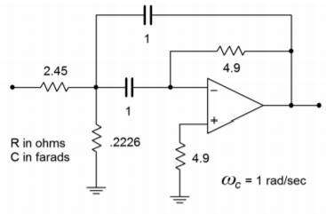
Figure \(\PageIndex{4}\): Initial damping calculation for Example \(\PageIndex{1}\).
The resulting normalized circuit is shown in Figure \(\PageIndex{4}\). We must now find the frequency scaling factor.
\[\omega_o = 2 \pi f_o \\ \omega_o = 2 \pi 980 Hz \\ \omega_o = 6158 \text{ radians per second} \nonumber \]
In order to translate our circuit to this frequency, we must divide either the resistors or the capacitors by 6158. In this example, let's use the capacitors.
\[C = \frac{1}{6158} \\ C = 162.4 \mu F \nonumber \]
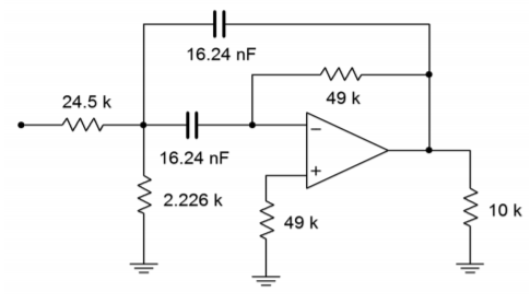
Figure \(\PageIndex{5}\): Final impedance and frequency scaling for Example \(\PageIndex{1}\).
A further impedance scaling is needed for practical component values. A factor of a few thousand or so would be appropriate here. To keep the calculations simple, we'll choose 10 k. Each resistor will be increased by 10 k, and each capacitor will be reduced by 10 k. The final scaled filter is shown in Figure \(\PageIndex{5}\).
Computer Simulation
The Multisim simulation of the circuit of Example \(\PageIndex{1}\) is shown in Figure \(\PageIndex{6}\). Note that the gain is 0 dB at the approximate center frequency (about 1 kHz). Also, the −3 dB breakpoints of 800 Hz and 1200 Hz are clearly seen. The phase response of this filter is also plotted. Note the very fast phase transition in the area around \(f_o\). If the \(Q\) of this circuit was increased, this transition would be faster still.
In simulations such as this, it is very important that realistic op amp models be employed. If an over-idealized version is used, non-ideal behavior due to a reduction of loop-gain will go unnoticed. This error is most likely to occur in circuits with high center frequencies and/or high \(Q\) s. You can verify this by translating the filter to a higher frequency and rerunning the simulation. For example, if \(C_1\) and \(C_2\) are decreased by a factor of 1000, the center frequency should move up to about 1 MHz. If the simulation is run again with an appropriate range of test frequencies, you will see that the limited bandwidth of the \(\mu\)A741 op amp prematurely cuts off the filter response. The result is a peaking frequency more than one octave below target, a maximum amplitude several dB below 0, and an asymmetrical response curve. This response graph is shown in Figure \(\PageIndex{6c}\). The accompanying phase plot also shows a great deviation from the ideal filter. An excessive phase shift at the middle and higher frequencies is clearly evident.
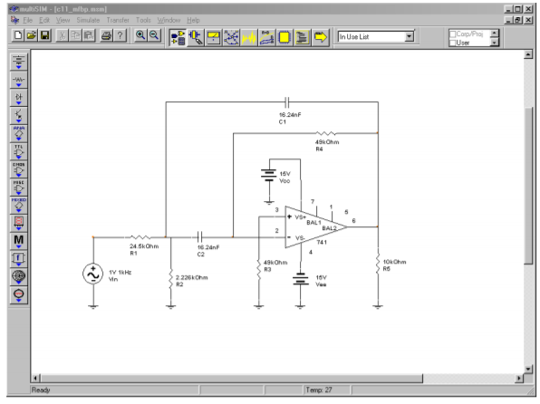
Figure \(\PageIndex{6a}\): Band-pass filter in Multisim.
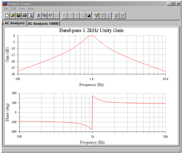
Figure \(\PageIndex{6b}\): Gain and phase plots for band-pass filter.
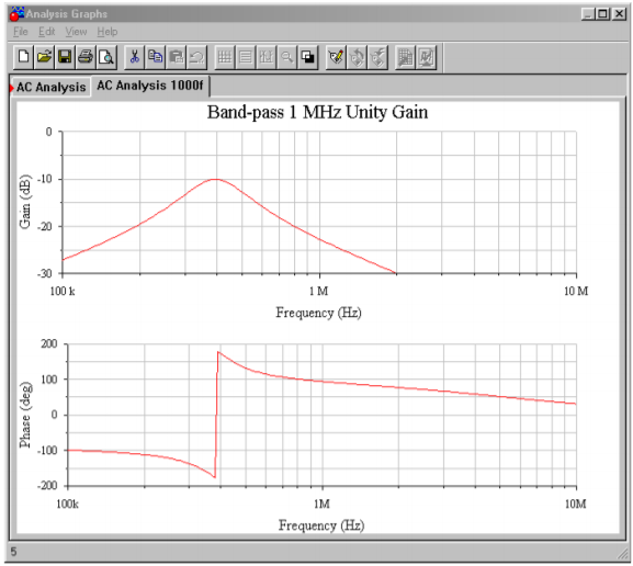
Figure \(\PageIndex{6c}\): Gain and phase plots for 1000 times frequency shift.
11.7.2: State-Variable Filter
As noted earlier, the multiple-feedback filter is not suited to high frequency or high \(Q\) work. For applications requiring \(Q\) s of about 10 or more, the state-variable filter is the form of choice. The state-variable is often referred to as the universal filter, as band-pass, high-pass, and low-pass outputs are all available. With additional components, a band-reject output may be formed as well. Unlike the earlier filter forms examined, the basic state-variable filter requires three op amps. Also, it is a second-order type, although higher-order types are possible. This form gets its name from state-variable analysis. One of the earliest uses for op amps was in the construction of analog computers (see Chapter Ten). Interconnections of differentiators, amplifiers, summers, and integrators were used to electronically solve differential equations that described physical systems. State-variable analysis provides a technique for solving involved differential equations. The equations may in fact, describe a required filter's characteristics. Although we will not examine state-variable analysis, this does not preclude a study of the state-variable filter. Designing with state-variable filters is really no more complex than our previous work.
Besides its ability to provide stable filters with relatively high \(Q\) s, the state-variable has other unique characteristics:
- It is relatively easy to tune electronically over a broad frequency range.
- It is possible to independently adjust the \(Q\) and tuning frequency.
- It offers the ability to create other, more complex, filters, as it has multiple outputs.
The state-variable filter is based on integrators. The general form utilizes a summing amplifier and two integrators, as shown in Figure \(\PageIndex{7}\). To understand how this circuit works on an intuitive level, recall that integrators are basically first-order, low-pass filters. As you can see, the extreme right side output has passed through the integrators and produces a low-pass response. If the low-pass output is summed out of phase with the input signal, the low frequency information will cancel, leaving just the high frequency components. Therefore, the output of the summer is the high-pass output of the filter. If the high-pass signal is integrated (using the same critical frequency), the result will be a band-pass response. This is seen at the output of the first integrator. The band-pass signal is also routed back to the input summing amplifier. By changing the amount of the signal that is fed back, the response near the critical frequency may be altered, effectively setting the filter \(Q\). Finally, the loop is completed by integrating the band-pass response, which yields the low-pass output. In effect, the second integrator's −6 dB per octave rolloff perfectly compensates for the rising band-pass response below \(f_o\). This produces flat response below \(f_o\). Above \(f_o\), the combination of the two falling response curves produces the expected second-order, low-pass response.
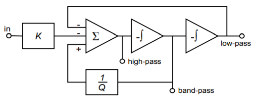
Figure \(\PageIndex{7}\): Block diagram of state-variable filter.
Two popular ways of configuring the state-variable filter are the fixed-gain and adjustable-gain forms. The fixed-gain form is shown in Figure \(\PageIndex{8}\). This circuit uses a total of three op amps. The \(Q\) of the circuit is set by a single resistor, \(R_Q\). \(Q\)s up to 100 are possible with state-variable filters. For the high- and low-pass outputs, the gain of this circuit is unity. For the band-pass output, the gain is equal to \(Q\).
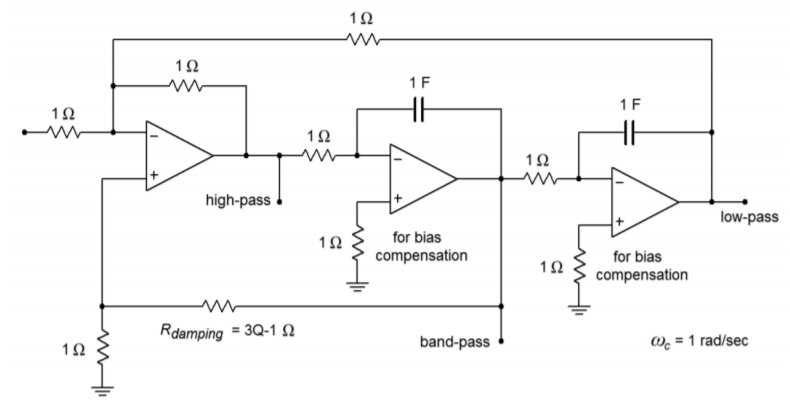
Figure \(\PageIndex{8}\): Fixed-gain version of state-variable filter.
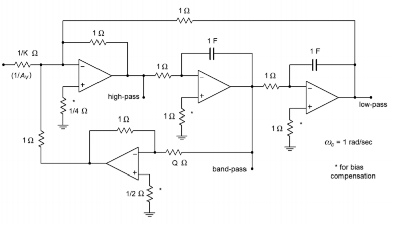
Figure \(\PageIndex{9}\): Variable-gain version of state-variable filter.
Figure \(\PageIndex{9}\) shows an adjustable-gain version. For high- or low-pass use, the gain is equal to the arbitrary value \(K\), whereas for band-pass use, the gain is equal to \(KQ\). This variation requires a fourth op amp in order to isolate the \(Q\) and gain settings. Although four op amps may sound like a large number of devices, remember that a variety of quad op amp packages exist, indicating that the actual physical layout may be quite small. Also, even though three different outputs are available, it is not possible to individually optimize each one for simultaneous use. Consequently, the state-variable is most often used as a stable and switchable high/low-pass filter, or as a high \(Q\) band-pass filter. Finally, in keeping with our previous work, the circuits are shown normalized to a critical frequency of one radian per second. Although we will concentrate on band-pass design in this section, it is possible to use these circuits to realize various high- and low-pass filters, such as those generated with the Sallen and Key forms. The procedure is nearly identical and uses the same frequency and damping factors (Figures 11.6.13 and 11.6.18).
Example \(\PageIndex{2}\)
Design a band-pass filter with a center frequency of 4.3 kHz and a \(Q\) of 25. Use the fixed-gain form.
First, determine the damping resistor value. Then, scale the components for the desired center frequency. Note that a \(Q\) of 25 produces a bandwidth of only 172 hertz for this filter (4.3 kHz/25).
\[R_{damping} = 3Q−1 \\ R_{damping} = 3 \times 25−1 \\ R_{damping} = 74 \Omega \nonumber \]
\[\omega_o = 2 \pi f_o \\ \omega_o = 2 \pi 4.3kHz \\ \omega_o = 27.02 k \text{ radians per second} \nonumber \]
In order to translate the filter to our desired center frequency, we need to divide either the resistors or the capacitors by 27,020. For this example, we'll use the capacitors.
\[C = \frac{1}{27.02 k} \\ C = 37 \mu F \nonumber \]
A final impedance scaling is required to achieve reasonable component values. A reasonable value might be a factor of 5000.
\[C = \frac{ 37 \mu F}{5000} \\ C = 7.4 nF \nonumber \]
\[R_{damping} = 74\times 5000 \\ R_{damping} = 370 k \Omega \nonumber \]
All remaining resistors will equal \(5 k\Omega\).
Because this is a band-pass filter,
\[A_v = Q \\ A_v = 25 \nonumber \]
The completed filter is shown in Figure \(\PageIndex{10}\). The value for \(R_{damping}\) is considerably larger than the other resistors. This effect gets worse as the required \(Q\) is increased. If this value becomes too large for practical components, it may be reduced to a more reasonable value as long as the associated divider resistor (from the noninverting input to ground) is reduced by the same amount. The ratio of these two resistors is what sets the filter \(Q\), not their absolute values. Lowering these values will upset the ideal input bias current compensation, but this effect can be ignored in many cases, or reduced through the use of FET input op amps.
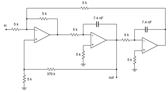
Figure \(\PageIndex{10}\): Completed design of bandpass filter for Example \(\PageIndex{2}\).
Altering this circuit for a variable-gain configuration requires the addition of a fourth amplifier as shown in Figure \(\PageIndex{9}\). The calculation for the damping resistor is altered, and a value for the input gain determining resistor is needed. The remaining component calculations are unchanged from the example above. Note that by setting the gain constant \(K\) to \(1/Q\), the final filter gain may be set to unity.