2.4: Special Cases of Lossless Terminated Lines
- Page ID
- 41015
\( \newcommand{\vecs}[1]{\overset { \scriptstyle \rightharpoonup} {\mathbf{#1}} } \)
\( \newcommand{\vecd}[1]{\overset{-\!-\!\rightharpoonup}{\vphantom{a}\smash {#1}}} \)
\( \newcommand{\id}{\mathrm{id}}\) \( \newcommand{\Span}{\mathrm{span}}\)
( \newcommand{\kernel}{\mathrm{null}\,}\) \( \newcommand{\range}{\mathrm{range}\,}\)
\( \newcommand{\RealPart}{\mathrm{Re}}\) \( \newcommand{\ImaginaryPart}{\mathrm{Im}}\)
\( \newcommand{\Argument}{\mathrm{Arg}}\) \( \newcommand{\norm}[1]{\| #1 \|}\)
\( \newcommand{\inner}[2]{\langle #1, #2 \rangle}\)
\( \newcommand{\Span}{\mathrm{span}}\)
\( \newcommand{\id}{\mathrm{id}}\)
\( \newcommand{\Span}{\mathrm{span}}\)
\( \newcommand{\kernel}{\mathrm{null}\,}\)
\( \newcommand{\range}{\mathrm{range}\,}\)
\( \newcommand{\RealPart}{\mathrm{Re}}\)
\( \newcommand{\ImaginaryPart}{\mathrm{Im}}\)
\( \newcommand{\Argument}{\mathrm{Arg}}\)
\( \newcommand{\norm}[1]{\| #1 \|}\)
\( \newcommand{\inner}[2]{\langle #1, #2 \rangle}\)
\( \newcommand{\Span}{\mathrm{span}}\) \( \newcommand{\AA}{\unicode[.8,0]{x212B}}\)
\( \newcommand{\vectorA}[1]{\vec{#1}} % arrow\)
\( \newcommand{\vectorAt}[1]{\vec{\text{#1}}} % arrow\)
\( \newcommand{\vectorB}[1]{\overset { \scriptstyle \rightharpoonup} {\mathbf{#1}} } \)
\( \newcommand{\vectorC}[1]{\textbf{#1}} \)
\( \newcommand{\vectorD}[1]{\overrightarrow{#1}} \)
\( \newcommand{\vectorDt}[1]{\overrightarrow{\text{#1}}} \)
\( \newcommand{\vectE}[1]{\overset{-\!-\!\rightharpoonup}{\vphantom{a}\smash{\mathbf {#1}}}} \)
\( \newcommand{\vecs}[1]{\overset { \scriptstyle \rightharpoonup} {\mathbf{#1}} } \)
\( \newcommand{\vecd}[1]{\overset{-\!-\!\rightharpoonup}{\vphantom{a}\smash {#1}}} \)
\(\newcommand{\avec}{\mathbf a}\) \(\newcommand{\bvec}{\mathbf b}\) \(\newcommand{\cvec}{\mathbf c}\) \(\newcommand{\dvec}{\mathbf d}\) \(\newcommand{\dtil}{\widetilde{\mathbf d}}\) \(\newcommand{\evec}{\mathbf e}\) \(\newcommand{\fvec}{\mathbf f}\) \(\newcommand{\nvec}{\mathbf n}\) \(\newcommand{\pvec}{\mathbf p}\) \(\newcommand{\qvec}{\mathbf q}\) \(\newcommand{\svec}{\mathbf s}\) \(\newcommand{\tvec}{\mathbf t}\) \(\newcommand{\uvec}{\mathbf u}\) \(\newcommand{\vvec}{\mathbf v}\) \(\newcommand{\wvec}{\mathbf w}\) \(\newcommand{\xvec}{\mathbf x}\) \(\newcommand{\yvec}{\mathbf y}\) \(\newcommand{\zvec}{\mathbf z}\) \(\newcommand{\rvec}{\mathbf r}\) \(\newcommand{\mvec}{\mathbf m}\) \(\newcommand{\zerovec}{\mathbf 0}\) \(\newcommand{\onevec}{\mathbf 1}\) \(\newcommand{\real}{\mathbb R}\) \(\newcommand{\twovec}[2]{\left[\begin{array}{r}#1 \\ #2 \end{array}\right]}\) \(\newcommand{\ctwovec}[2]{\left[\begin{array}{c}#1 \\ #2 \end{array}\right]}\) \(\newcommand{\threevec}[3]{\left[\begin{array}{r}#1 \\ #2 \\ #3 \end{array}\right]}\) \(\newcommand{\cthreevec}[3]{\left[\begin{array}{c}#1 \\ #2 \\ #3 \end{array}\right]}\) \(\newcommand{\fourvec}[4]{\left[\begin{array}{r}#1 \\ #2 \\ #3 \\ #4 \end{array}\right]}\) \(\newcommand{\cfourvec}[4]{\left[\begin{array}{c}#1 \\ #2 \\ #3 \\ #4 \end{array}\right]}\) \(\newcommand{\fivevec}[5]{\left[\begin{array}{r}#1 \\ #2 \\ #3 \\ #4 \\ #5 \\ \end{array}\right]}\) \(\newcommand{\cfivevec}[5]{\left[\begin{array}{c}#1 \\ #2 \\ #3 \\ #4 \\ #5 \\ \end{array}\right]}\) \(\newcommand{\mattwo}[4]{\left[\begin{array}{rr}#1 \amp #2 \\ #3 \amp #4 \\ \end{array}\right]}\) \(\newcommand{\laspan}[1]{\text{Span}\{#1\}}\) \(\newcommand{\bcal}{\cal B}\) \(\newcommand{\ccal}{\cal C}\) \(\newcommand{\scal}{\cal S}\) \(\newcommand{\wcal}{\cal W}\) \(\newcommand{\ecal}{\cal E}\) \(\newcommand{\coords}[2]{\left\{#1\right\}_{#2}}\) \(\newcommand{\gray}[1]{\color{gray}{#1}}\) \(\newcommand{\lgray}[1]{\color{lightgray}{#1}}\) \(\newcommand{\rank}{\operatorname{rank}}\) \(\newcommand{\row}{\text{Row}}\) \(\newcommand{\col}{\text{Col}}\) \(\renewcommand{\row}{\text{Row}}\) \(\newcommand{\nul}{\text{Nul}}\) \(\newcommand{\var}{\text{Var}}\) \(\newcommand{\corr}{\text{corr}}\) \(\newcommand{\len}[1]{\left|#1\right|}\) \(\newcommand{\bbar}{\overline{\bvec}}\) \(\newcommand{\bhat}{\widehat{\bvec}}\) \(\newcommand{\bperp}{\bvec^\perp}\) \(\newcommand{\xhat}{\widehat{\xvec}}\) \(\newcommand{\vhat}{\widehat{\vvec}}\) \(\newcommand{\uhat}{\widehat{\uvec}}\) \(\newcommand{\what}{\widehat{\wvec}}\) \(\newcommand{\Sighat}{\widehat{\Sigma}}\) \(\newcommand{\lt}{<}\) \(\newcommand{\gt}{>}\) \(\newcommand{\amp}{&}\) \(\definecolor{fillinmathshade}{gray}{0.9}\)The lossless transmission line configurations considered in this section are used as circuit elements in RF designs and are used elsewhere in this book series. The first element considered in Section 2.4.1 is a short length of short-circuited line which looks like an inductor. The element considered in Section 2.4.2 is a short length of open-circuited line which looks like a capacitor. Then lengths of short-circuited and open-circuited lines, called stubs, used nearly always as shunt elements to introduce an admittance in a circuit, are described in Sections 2.4.3 and 2.4.4. Another type of element, described in Section 2.4.5, is a short length of line with either high or low characteristic impedance realizing a small series inductor or capacitor respectively. The final element described in Section 2.4.6 is a quarter-wave transformer, a quarter-wavelength long line with a particular characteristic impedance which is used in two ways. It can be used to provide maximum power transfer from a source to a load resistance, and it can invert an impedance, e.g. making a capacitor terminating the line look like an inductor.
2.4.1 Short Length of Short-Circuited Line
A transmission line terminated in a short circuit (\(Z_{L} = 0\)) has the input impedance (using Equation (2.3.18))
\[\label{eq:1}Z_{\text{in}}=\jmath Z_{0}\tan(\beta\ell) \]
So a short length of line, \(\ell<\lambda_{g}/4\), looks like an inductor with inductance \(L_{s}\),
\[\label{eq:2}Z_{0}\tan(\beta\ell)=\omega L_{s},\quad\text{and so}\quad L_{s}=\frac{Z_{0}}{\omega}\tan\frac{2\pi\ell}{\lambda_{g}} \]
From Equation \(\eqref{eq:2}\) it can be seen that for a given \(\ell\), \(L_{s}\) is proportional to \(Z_{0}\). Hence, for larger values of \(L_{s}\), sections of transmission line of high characteristic impedance are needed. So microstrip lines with narrow strips can be used to realize inductors in planar microstrip circuits.
2.4.2 Short Length of Open-Cicuited Line
An open-circuited line has \(Z_{L} = ∞\) and so (using Equation (2.3.18))
\[\label{eq:3}Z_{\text{in}}=-\jmath\frac{Z_{0}}{\tan\beta\ell} \]
For lengths \(\ell\) such that \(\ell < \lambda/4\), an open-circuited segment of line realizes a capacitor \(C_{0}\) for which
\[\label{eq:4}\frac{1}{\omega C_{0}}=\frac{Z_{0}}{\tan\beta\ell}\quad\text{and so}\quad C_{0}=\frac{1}{Z_{0}}\frac{\tan(\beta\ell)}{\omega} \]
From the above relationship, it can be seen that \(C_{0}\) is inversely proportional to \(Z_{0}\). Hence, for larger values of \(C_{0}\), sections of transmission line with low characteristic impedance need to be used.
2.4.3 Short-Circuited Stub
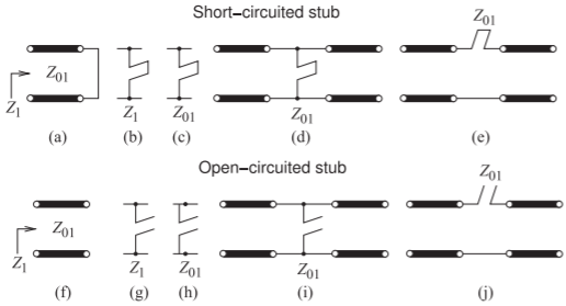
A stub is a section of open-circuited or short-circuited transmission line and is used as a series or shunt element in a microwave circuit. There are several representations. A shorted stub is shown in Figure \(\PageIndex{1}\)(a) as a transmission line with characteristic impedance \(Z_{01}\) that is short circuited. The input impedance of the line is \(Z_{1}\). If the line is lossless, the usual assumption, then \(Z_{01}\) will be real and \(Z_{1}\) will be imaginary. Stubs are commonly used in microwave circuits and generally all stubs in a network have the same length, such as \(\lambda/4\) long or \(\lambda/8\) long. Which it is is specified in the design. Realistically they do not need to have the same length but there are some special properties for certain lengths, as will become clearer. A cleaner way to indicate a shorted stub is shown in Figure \(\PageIndex{1}\)(b), where the value of the stub is as indicated. The absence of a \(0\) subscript (which would indicate

Figure \(\PageIndex{1}\): Transmission line stubs: (a)–(e) short-circuited stubs; and (f)–(j) open-circuited stubs.
characteristic impedance) means that this is the reactive input impedance of the stub. If a \(0\) subscript is used, as in Figure \(\PageIndex{1}\)(c), the characteristic impedance of the stub is indicated. If a numerical value is given then an imaginary impedance indicates that the input impedance is being specified, whereas a real impedance indicates the characteristic impedance of the stub. The shorted stub is shown as a shunt element in Figure \(\PageIndex{1}\)(d) and as a series element in Figure \(\PageIndex{1}\)(e). However in nearly all transmission line technologies, including microstrip, only shunt stubs can be realized. The open-circuited stubs with annotations are shown in Figures \(\PageIndex{1}\)(f–j) with similar assignments of meaning. The length of a stub is often indicated by its resonant frequency, \(f_{r}\). This is the frequency at which the stub is \(\lambda/4\) long.
The shorted stub in Figure \(\PageIndex{1}\)(a) has the input impedance (from Equation (2.3.18))
\[\label{eq:5}Z_{1}=\jmath Z_{01}\tan\beta\ell \]
where \(\ell\) is the physical length of the line. Since the stub is \(\lambda/4\) long at \(f_{r}\), then at frequency \(f\), the input impedance of the stub is
\[\label{eq:6}Z_{1}=\jmath Z_{01}\tan\left(\frac{\pi}{2}\frac{f}{f_{r}}\right) \]
A special situation, and the most commonly used in design, is when the operating frequency is around one-half of the resonant frequency (i.e., \(f\approx\frac{1}{2}f_{r}\)). Then the stub is one-eighth of a wavelength long and the argument of the tangent function in Equation \(\eqref{eq:6}\) is approximately \(π/4\) and \(Z_{1}\) becomes
\[\label{eq:7}Z_{1}\approx\jmath Z_{01}\tan\left(\frac{\pi}{4}\right)=\jmath Z_{01} \]
thus realizing an inductance at \(f = f_{r}/2\) with a reactance equal to the characteristic impedance of the line.
Develop the electrical design of the shunt stub shown with a load of impedance \(Z_{L} = 75 +\jmath 15\:\Omega\) so that the total impedance of the load and stub is real.

Figure \(\PageIndex{2}\)
Solution
The short-circuited stub has characteristic impedance \(Z_{01}\) and length \(\ell_{1}\). Choose \(Z_{01} = 75\:\Omega\) (generally this must be between \(15\:\Omega\) and \(100\:\Omega\) for most transmission line technologies). The stub needs to be designed so that the susceptances of the stub and load sum to zero. The admittance of the load \(Y_{L} = 1/Z_{L} = 0.01282 −\jmath 0.002564\text{ S}\). The required admittance of the stub is \(Y_{\text{STUB}} =\jmath 0.002564\text{ S}\) so, using Equation \(\eqref{eq:5}\),
\[Z_{\text{STUB}}=1/Y_{\text{STUB}}=\jmath Z_{01}\tan\beta\ell_{1}=-\jmath 390\:\Omega\nonumber \]
Therefore, the electrical length of the stub is
\[\label{eq:8}\beta\ell_{1}=\arctan(-\jmath 390/\jmath 75)=-1.381+n\pi\text{ radians},\:n=0,1,2,\ldots \]
The first positive angle is taken so the stub has the shortest length. So
\[\label{eq:9}\beta\ell_{1}=1.761\text{ radians}=100.9^{\circ} \]
The complete electrical design of the stub is that it is a shunt short-circuited stub with a characteristic impedance of \(75\:\Omega\) and with an electrical length of \(100.9^{\circ}\). The combined impedance of the stub and load is \(Z_{X} = 1/(\Re\{Y_{L}\})=1/0.01282 = 78.00\:\Omega\).
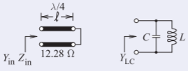
This example presents an analytic approach to developing the equivalent circuit of a shorted stub at resonance. Consider a shorted transmission line with characteristic impedance \(Z_{0} = 12.28\:\Omega\) and resonant, i.e. a quarter-wavelength long, at \(1850\text{ MHz}\).
Solution
At the first resonant frequency, \(f_{r} =\omega_{r}/(2π)\), the transmission line presents an open circuit and the appropriate circuit model is shown on the right.

Figure \(\PageIndex{3}\)
The strategy here is to develop the \(LC\) equivalent circuit by equating the derivatives of the resonator and the \(LC\) circuit. This is in addition to equating the input admittances of the two circuits at the resonant frequency \(f_{r} = \omega_{r}/(2π)\). That is, at frequency \(f_{r}\)
\[\label{eq:10} Y_{\text{in}}(f_{r})=0=Y_{LC}(f_{r})=\jmath[\omega_{r}C-1/(\omega_{r}L)]\quad\text{and so}\quad\omega_{r}^{2}=1/(LC) \]
The input impedance of the line at frequency \(f = \omega/(2π)\) is \(Z_{\text{in}}(\omega) = \jmath Z_{0} \tan (\beta\ell)\), and so its input admittance is
\[\label{eq:11}Y_{\text{in}}(\omega)=\frac{-\jmath}{Z_{0}}\cot(\beta\ell) \]
The derivative of the transmission line admittance is (using Equation (1.A.26))
\[\label{eq:12}\frac{\partial Y_{\text{in}}}{\partial\omega}=\frac{\partial\beta\ell}{\partial\omega}\frac{\partial Y_{\text{in}}}{\partial\beta\ell}=\frac{\partial\beta\ell}{\partial\omega}\left(\frac{-\jmath}{Z_{0}}\right)[-\csc^{2}(\beta\ell)] \]
Now \(\beta\) is proportional to \(\omega\) for a lossless dispersionless line so
\[\frac{\partial Y_{\text{in}}}{\partial\omega}=\frac{\beta\ell}{\omega}\frac{\jmath}{Z_{0}}\csc^{2}(\beta\ell)\nonumber \]
Since the line is approximately \(\lambda/4\) long near the resonant frequency, for \(f\approx f_{r},\:\beta\ell\approx π/2,\: \csc(\beta\ell)\approx 1\) (which is a good approximation since at \(f_{r}\), \([\partial \csc(\beta\ell)]/(\partial\omega) = 0\)), and
\[\label{eq:13}\left.\frac{\partial Y_{\text{in}}}{\partial\omega}\right|_{\omega_{r}}=\frac{\jmath\beta\ell}{\omega_{r}Z_{0}} \]
The input admittance of the parallel \(LC\) circuit is
\[\label{eq:14}Y_{LC}=\jmath\left(\omega C-\frac{1}{\omega L}\right)\quad\text{and}\quad\frac{\partial Y_{LC}}{\partial\omega}=\jmath\left( C+\frac{1}{\omega^{2}L}\right) \]
At and near resonance \(\omega^{2}\approx 1/(LC)\) and so
\[\label{eq:15}\left.\frac{\partial Y_{\text{LC}}}{\partial\omega}\right|_{\omega_{r}}=\jmath 2C \]
Equating the derivatives of \(Y_{\text{in}}\), Equation \(\eqref{eq:13}\), and of \(Y_{\text{LC}}\), Equation \(\eqref{eq:15}\), yields
\[\label{eq:16}\frac{-\jmath\beta\ell}{\omega Z_{0}}=\jmath 2C \]
Thus (since \(\beta\ell\approx\pi/2\))
\[\label{eq:17}C=\frac{\pi}{4\omega_{r}Z_{0}}=\frac{\pi}{4\cdot 2\pi\cdot 1850\cdot 10^{6}\cdot 12.28}=5.502\cdot 10^{-12}\text{ F}=5.502\text{ pF} \]
and, since \(\omega_{r}^{2} = 1/(LC)\),
\[\label{eq:18}L=\frac{1}{\omega_{r}^{2}C}=\frac{1}{(2\pi\cdot 1850\cdot 10^{6})^{2}\cdot 5.502\cdot 10^{-12}}=1.345\cdot 10^{-9}\text{ H}=1.345\text{ nH} \]
2.4.4 Open-Circuited Stub
An open-circuited transmission line is commonly used as a circuit element called an open stub shown in Figure \(\PageIndex{1}\)(f–j). From Equation (2.3.18) and noting that \(Z_{L} = ∞\), the open stub input impedance is
\[\label{eq:19}Z_{1}=-\jmath Z_{01}\frac{1}{\tan\beta\ell} \]
With the stub one-quarter wavelength long at the frequency \(f_{r}\), the input impedance at \(f_{r}\) is a short circuit and the stub is said to be resonant at \(f_{r}\). Then at a frequency \(f\), the input impedance of the stub is
\[\label{eq:20}Z_{1}=-\jmath Z_{01}\tan^{-1}\left(\frac{\pi}{2}\frac{f}{f_{r}}\right) \]
When \(f = \frac{1}{2}f_{r}\) the stub is one-eighth wavelength long and
\[\label{eq:21}Z_{1}=-\jmath Z_{01}\frac{1}{\tan\left(\frac{\pi}{4}\right)}=-\jmath Z_{01} \]
So a \(\lambda/8\) long open-circuited stub (\(\lambda/4\) at \(f_{r}\), \(f =\frac{1}{2}f_{r}\)) realizes a capacitance with a reactance equal to the characteristic impedance of the line.
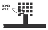
If the length of a stub can be changed then the stub can be used as a tuning element. A common microstrip tuning technique is shown in Figure \(\PageIndex{4}\), where bonding to different pads enables a variable length stub to be realized.

Figure \(\PageIndex{4}\): Open-circuited stub with variable length realized using wire bonding from the fixed stub to one of the bond pads. The bond pads are on the same layer as the strip metal layer and bonding to them extends the length of the open-circuited stub.
Develop the electrical design of the open-circuit stub shown with a load of impedance \(Z_{L} = 75 +\jmath 15\:\Omega\) so that the total impedance of the load and stub is real.

Figure \(\PageIndex{5}\)
Solution
The open-circuited stub has characteristic impedance \(Z_{01}\) and length \(\ell_{1}\). A good choice is to choose \(Z_{01}\) around the impedance level of the load as long as it can be realized; so choose \(Z_{01} = 75\:\Omega\). The stub needs to be designed so that the susceptances of the stub and load sum to zero. The admittance of the load \(Y_{L} = 1/Z_{L} = 0.01282 −\jmath 0.002564\text{ S}\). The required admittance of the stub is \(Y_{\text{STUB}} = \jmath 0.002564\text{ S}\), so, using Equation \(\eqref{eq:19}\),
\[Z_{\text{STUB}}=1/Y_{\text{STUB}}=-\jmath Z_{01}/\tan\beta\ell_{1}=-\jmath 390\:\Omega\nonumber \]
Therefore, the electrical length of the stub is
\[\label{eq:22}\beta\ell_{1}=\arctan(\jmath 75/\jmath 390)=0.1900+n\pi\text{ radians},n=0,1,2,\ldots \]
The first positive angle is taken so the stub has the shortest length. Then
\[\label{eq:23}\beta\ell_{1}=0.1900\text{ radians}=10.89^{\circ} \]
The complete electrical design of the stub is that it is a shunt open-circuited stub with a characteristic impedance of \(75\:\Omega\) and an electrical length of \(10.89^{\circ}\). The combined impedance of the stub and load is \(Z_{X} = 1/(\Re\{Y_{L}\})=1/0.01282 = 78.00\:\Omega\).
2.4.5 Electrically Short Lossless Line
Consider the input impedance, \(Z_{\text{in}}\), of an electrically short line (i.e., \(\beta\ell\) is small) (see Figure \(\PageIndex{6}\)). Using Equation (2.3.18),
\[\label{eq:24}Z_{\text{in}}\approx\frac{Z_{L}+\jmath Z_{0}(\beta\ell)}{1+\jmath(Z_{L}/Z_{0})(\beta\ell)}\approx [Z_{L}+\jmath Z_{0}(\beta\ell)]\left[1-\jmath\frac{Z_{L}}{Z_{0}}(\beta\ell)\right] \]
Since \(Z_{0}\beta = \sqrt{L/C}(\omega\sqrt{LC}) = \omega L\) and \(\beta/Z_{0} = (\omega\sqrt{LC})/\sqrt{L/C}) = \omega C\) (where \(L\) and \(C\) are the inductance and capacitance per unit length of the line), Equation \(\eqref{eq:24}\) can be written as
\[\label{eq:25}Z_{\text{in}}\approx Z_{L}\left[1+(\beta\ell)^{2}\right]+\jmath\left[\omega(L\ell)-Z_{L}^{2}\omega(C\ell)\right] \]
Since \(\beta\ell\) is small, \((\beta\ell)^{2}\) is very small, and so the \((\beta\ell)^{2}\) term can be ignored. Then the input impedance of an electrically short line terminated in impedance \(Z_{L}\) is
\[\label{eq:26}Z_{\text{in}}\approx Z_{L}+\jmath[\omega(L\ell)-Z_{L}^{2}\omega(C\ell)] \]
Some special cases of this result will be considered in the following examples.

Figure \(\PageIndex{6}\): An electrically short line.
This example demonstrates that a predominantly capacitive behavior can be obtained from a short segment of transmission line, the \(Z_{01}\) line here, of low characteristic impedance. Consider the transmission line system shown below with lines having the characteristic impedances, \(Z_{01}\) and \(Z_{02}\), \(Z_{02} ≫ Z_{01}\).

Figure \(\PageIndex{7}\)
The value of \(Z_{\text{in}}\) is (treating \(Z_{02}\) as the load)
\[\label{eq:27}Z_{\text{in}}=Z_{01}\frac{Z_{02}+\jmath Z_{01}\tan\beta\ell}{Z_{01}+\jmath Z_{02}\tan\beta\ell} \]
Now \((1 +\jmath x)^{−1}\approx 1 −\jmath x − x^{2}\). Thus for a short line (and so dropping the \(\tan^{2}(\beta\ell)\) term)
\[\label{eq:28}Z_{\text{in}}\approx Z_{02}-\jmath\frac{Z_{02}^{2}}{Z_{01}}\tan(\beta\ell)+\jmath Z_{01}\tan(\beta\ell)=Z_{02}+\jmath Z_{01}\tan(\beta\ell)\left[1-\frac{Z_{02}^{2}}{Z_{01}^{2}}\right] \]
For \(Z_{02} ≫ Z_{01}\) and for a short line, \(\tan(\beta\ell)\approx\beta\ell\), and this becomes
\[\label{eq:29}Z_{\text{in}}\approx Z_{02}-\jmath\frac{Z_{02}^{2}}{Z_{01}}\tan(\beta\ell)\approx Z_{02}-\jmath\frac{Z_{02}^{2}}{Z_{01}}\beta\ell \]
which is capacitive. Now consider the circuit to the right where an effective capacitance \(C_{\text{eff}}\) is in shunt with a load \(Z_{02}\). This has the input impedance

Figure \(\PageIndex{8}\)
\[\label{eq:30}Z_{x}=\left(\jmath\omega C_{\text{eff}}+\frac{1}{Z_{02}}\right)^{-1}=\frac{Z_{02}}{1+\jmath\omega C_{\text{eff}}Z_{02}}=Z_{02}[1-\jmath\omega C_{\text{eff}}Z_{02}-(\jmath\omega C_{\text{eff}}Z_{02})^{2}\ldots \]
For \(\omega C_{\text{eff}} Z_{02} ≪ 1\) (i.e. an electrically short line)
\[\label{eq:31}Z_{x}\approx Z_{02}-\jmath\omega C_{\text{eff}}Z_{02}^{2} \]
Equating Equations \(\eqref{eq:29}\) and \(\eqref{eq:31}\), the effective value of the shunt capacitor realized by the short length of low-impedance line, the \(Z_{01}\) line, is
\[\label{eq:32}C_{\text{eff}}=\frac{1}{\omega Z_{02}^{2}}\frac{Z_{02}^{2}\beta\ell}{Z_{01}}=\frac{\beta}{\omega}\frac{\ell}{Z_{01}} \]
Thus a shunt capacitor can be realized approximately by a low-impedance line embedded between two highimpedance lines. The microstrip layout of this is shown in the figure on the right. Recall that a wide microstrip line has a low characteristic impedance.

Figure \(\PageIndex{9}\)
This example demonstrates that a (predominantly) inductive behavior can be obtained from a segment of transmission line. Consider the transmission line system shown below with lines having two different characteristic impedances, \(Z_{01}\) and \(Z_{02}\), \(Z_{02} ≪ Z_{01}\).

Figure \(\PageIndex{10}\)
The value of \(Z_{\text{in}}\) is (using Equation (2.3.18))
\[\label{eq:33}Z_{\text{in}}=Z_{01}\frac{Z_{02}+\jmath Z_{01}\tan\beta\ell}{Z_{01}+\jmath Z_{02}\tan\beta\ell} \]
which for a short line can be expressed as
\[\label{eq:34}Z_{\text{in}}\approx Z_{02}[1+\tan(\beta\ell)]+\jmath Z_{01}\tan(\beta\ell) \]
Note that \(\jmath Z_{01}\tan(\beta\ell)\) is the dominant part for \(\ell < \lambda/8\) and \(Z_{02} ≪ Z_{01}\).
Thus a microstrip realization of a series inductor is a high-impedance line embedded between two low-impedance lines. A top view of such a configuration in microstrip is shown in the figure. A narrow microstrip line has high characteristic impedance.

Figure \(\PageIndex{11}\)
The previous two examples showed how a shunt capacitance or series inductance can be realized using short sections of line, the \(Z_{01}\) line here, with low or high characteristic impedance respectively. This enables realization of some lumped element circuits in microstrip form. A lumped element lowpass filter is shown in Figure \(\PageIndex{12}\)(a) and this can be realized using wide and narrow microstrip lines, as shown in Figure \(\PageIndex{12}\)(b).
2.4.6 Quarter-Wave Transformer
Figure \(\PageIndex{13}\)(a) shows a resistive load \(R_{L}\) and a section of transmission line with length \(\ell = \lambda_{g}/4\) (hence the name quarter-wave transformer). The input

Figure \(\PageIndex{12}\): A lowpass filter: (a) in the form of an \(LC\) ladder network; and (b) realized using microstrip lines.

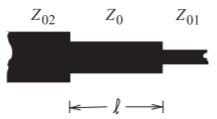
Figure \(\PageIndex{13}\): The quarter-wave transformer line: (a) transforming a load; and (b) interfacing two lines.

Figure \(\PageIndex{14}\): Layout of a microstrip quarter-wave transformer.
impedance of the line is
\[\label{eq:35}Z_{\text{in}}=Z_{1}\frac{R_{L}+\jmath Z_{1}\tan(\beta\ell)}{Z_{1}+\jmath R_{L}\tan(\beta\ell)}=Z_{1}\frac{R_{L}+\jmath Z_{1}\infty}{Z_{1}+\jmath R_{L}\infty}=\frac{Z_{1}^{2}}{R_{L}} \]
The input impedance is matched to the transmission line \(Z_{0}\) if
\[\label{eq:36}Z_{\text{in}}=Z_{0}^{\ast}=Z_{0} \]
since here the characteristic impedance is real. Thus
\[\label{eq:37}Z_{1}=\sqrt{Z_{0}R_{L}} \]
and so the one-quarter wavelength long line acts as an ideal impedance transformer.
Another example of the quarter-wave transformer is shown in Figure \(\PageIndex{13}\)(b). The input impedance looking into the quarter-wave transformer (from the left) is given by
\[\label{eq:38}Z_{\text{in}}=Z_{0}\frac{Z_{01}+\jmath Z_{0}\tan(\beta\ell)}{Z_{0}+\jmath Z_{01}\tan(\beta\ell)}=Z_{0}\frac{Z_{01}+\jmath Z_{0}\infty}{Z_{0}+\jmath Z_{01}\infty}=\frac{Z_{0}^{2}}{Z_{01}} \]
Hence a section of transmission line of length \(\ell = \lambda_{g}/4 + n\lambda_{g}/2\), where \(n = 0, 1, 2,\ldots,\) can be used to match lines having different impedances, \(Z_{01}\) and \(Z_{02}\), by constructing the line so that its characteristic impedance is
\[\label{eq:39}Z_{0}=\sqrt{Z_{01}Z_{02}} \]
Note that for a design center frequency \(f_{0}\), the matching section provides a perfect match only at the center frequency and at frequencies where \(\ell = \lambda_{g}/4 + n\lambda_{g}/2\).
The layout of a microstrip quarter-wave transformer is shown in Figure \(\PageIndex{14}\), where \(\ell = \lambda_{g}/4\) and the characteristic impedance of the transformer, \(Z_{0}\), is the geometric mean of the impedances on either side, that is, \(Z_{0} = \sqrt{Z_{01}Z_{02}}\).
A quarter-wave transformer has an interesting property that is widely used. Examine the final result in Equation \(\eqref{eq:38}\), which is repeated here:
\[\label{eq:40}Z_{\text{in}}=\frac{Z_{0}^{2}}{Z_{01}} \]
Equation \(\eqref{eq:40}\) indicates that a one-quarter wavelength long line is an impedance inverter presenting, at Port 1, the inverse of the impedance presented at port 2, \(Z_{01}\). This result also applies to complex impedances replacing \(Z_{01}\). This impedance inversion is scaled by the square of the characteristic impedance of the line. This inversion holds in the reverse direction as well.
2.4.7 Summary
The lossless transmission line configurations considered in this section are those most commonly used in microwave circuit design. It is important to note that the stub line is almost always used in shunt configuration to provide an admittance in a circuit. Most transmission line technologies, including coaxial lines and microstrip, only permit shunt stubs. The quarterwave transformer is a particularly interesting element enabling maximum power transfer from a source to a load that may be different. An interesting feature that is widely exploited is that the quarter-wave transformer inverts an impedance. For example, turning a small resistance into a large resistance, or even turning a small capacitor into a large inductance. These transformations are valid over a moderate bandwidth.


