
3.2: Substrates
- Page ID
- 41026

Planar transmission line design involves choosing both the transmission line structure to use and the substrate. In this section the electrical properties of materials will be discussed and then substrates commonly used with planar interconnects will be considered.
3.2.1 Dielectric Effect
The presence of material between the conductors alters the electrical characteristics of the interconnect. With a dielectric, the application of an electric field moves the centers of positive and negative charge at the atomic and molecular level. Moving the charge centers changes the amount of energy stored in the electric field—a process akin to storing energy in a stretched spring. The extra energy storage property is described by the relative permittivity, \(\varepsilon_{r}\), which is the ratio of the permittivity of the material to that of free space:
\[\label{eq:1}\varepsilon_{r}=\varepsilon/\varepsilon_{0} \]
The relative permittivities of materials commonly used with interconnects range from \(2.08\) for Teflon\(^{\text{TM}}\), used in high-performance PCBs and coaxial cables, to \(11.9\) for silicon (Si), to \(3.8–4.2\) for silicon dioxide (SiO\(_{2}\)), and \(12.4\) for gallium arsenide (GaAs).
When the fields are in more than one medium (a nonhomogeneous transmission line), as for the microstrip line, the effective relative permittivity, \(\varepsilon_{r,e}\) (or usually just \(\varepsilon_{e} = \varepsilon_{r,e}\)), is used. The characteristics of the nonhomogeneous line are then more or less the same as for the same structure with a uniform dielectric of permittivity, \(\varepsilon_{\text{eff}} = \varepsilon_{e}\varepsilon_{0}\). The \(\varepsilon_{\text{eff}}\) changes with frequency as the proportion of energy stored in the different regions changes. This effect is called dispersion and causes a pulse to spread out as the different frequency components of the pulse want to travel at different speeds.
3.2.2 Dielectric Loss Tangent, \(\tan\delta\)
Loss in a dielectric comes from two sources: (a) dielectric damping (also called dielectric relaxation) and (b) conduction losses in the dielectric. Dielectric damping originates from the movement of charge centers resulting in mechanical distortion of the dielectric lattice. An alternating electric field results in vibrational (or phonon) energy in the dielectric, thus energy is lost from the electric field. It is easy to see that this loss increases linearly with frequency and is zero at DC. Because of this, in the frequency domain loss is described by incorporating an imaginary term in the permittivity. So now the permittivity of a dielectric becomes
\[\label{eq:2}\varepsilon=\varepsilon_{r}\varepsilon_{0}=\varepsilon'-\jmath\varepsilon''=\varepsilon_{0}(\varepsilon_{r}'-\jmath\varepsilon_{r}'') \]
If there is no dielectric damping loss, \(\varepsilon''= 0\). The other type of loss that occurs in the dielectric is due to the movement of charge carriers in the dielectric. The ability to move charges is described by the conductivity, \(\sigma\), and the loss due to current conduction is independent of frequency. So the energy lost in the dielectric is proportional to \(\omega\varepsilon'' +\sigma\) and the energy stored in the electric field is proportional to \(\omega\varepsilon'\). Thus a loss tangent is introduced:
\[\label{eq:3}\tan\delta=\frac{\omega\varepsilon''+\sigma}{\omega\varepsilon'} \]
Also the relative permittivity can be redefined as
\[\label{eq:4}\varepsilon_{r}=\varepsilon_{r}'-\jmath\left(\varepsilon_{r}''+\frac{\sigma}{\omega\varepsilon_{0}}\right) \]
With the exception of silicon, the loss tangent is very small for dielectrics that are useful at RF and microwave frequencies and so most of the time
\[\label{eq:5}|\varepsilon_{r}|\approx\varepsilon_{r}' \]
and this is what is quoted as the permittivity of a material. Thus
\[\label{eq:6}\varepsilon_{r}=\varepsilon_{r}'-\jmath(\varepsilon_{r}''+\sigma/(\omega\varepsilon_{0}))\approx\varepsilon_{r}'(1-\jmath\tan\delta) \]
3.2.3 Magnetic Material Effect
A similar effect on energy storage in the magnetic field occurs for a few materials. The magnetic properties of materials are due to the magnetic dipole moments that result from alignment of electron spins—an intrinsic property of electrons. In most materials the electron spins occur in pairs with opposite signs, with the result that there is no net magnetic moment. However, in magnetic materials, some of the electron spins are not canceled and there is a net magnetic moment. This net magnetic moment aligns itself with an applied \(H\) field and so provides a mechanism for additional storage of magnetic energy. The relative permeability, \(\mu_{r}\), describes this effect and
\[\label{eq:7}\mu=\mu_{r}\mu_{0} \]
Most materials have \(\mu_{r} = 1\). One notable exception is nickel, which has a high permeability, is a very convenient processing material, and is often used in electronic packaging for its desirable processing properties.
As with dielectrics, the effect of loss in a magnetic material can be described by its complex permeability:
\[\label{eq:8}\mu=\mu'-\jmath\mu'' \]
Lossy magnetic effects are due to the movement of magnetic dipoles, which creates vibrations in a material and hence loss.
3.2.4 Substrates for Planar Transmission Lines
The properties of a number of common substrate materials are given in Table \(\PageIndex{1}\); more are given in Appendix 2.A. Crystal substrates such as sapphire, quartz, and semiconductors (Si, GaAs, and InP) have very good dimensional tolerances and uniformity of electrical properties. Many other substrates have high surface roughness and electrical properties that can vary. For example, FR4 is the most common type of printed circuit board substrate and is a weave of fiberglass embedded in resin. So the material is not uniform and in the assembly of a multilayer circuit board layers of FR4 are pressed together and the resin flows so that there is an unpredictable localized variation in the proportion of resin and glass. High-performance FR4 for microwave applications has a fine weave.
| Material | \(10^{4}\tan\delta\:\varepsilon_{r}\) (at \(10\text{ GHz}\)) | |
|---|---|---|
| Air (dry) | \(\approx 0\) | \(1\) |
| Alumina, \(99.5\%\) | \(1-2\) | \(10.1\) |
| Sapphire | \(0.4-0.7\) | \(9.4,\: 11.6\) |
| Glass, typical | \(20\) | \(5\) |
| Polyimide | \(50\) | \(3.2\) |
| Quartz (fused) | \(1\) | \(3.8\) |
| FR4 circuit board | \(100\) | \(4.3-4.5\) |
| RT-duroid 5880 | \(5-15\) | \(2.16-2.24\) |
| RT-duroid 6010 | \(10-60\) | \(10.2-10.7\) |
| AT-1000 | \(20\) | \(10.0-13.0\) |
| Si (high resistivity) | \(10-100\) | \(11.9\) |
| GaAs | \(6\) | \(12.85\) |
| InP | \(10\) | \(12.4\) |
| SiO\(_{2}\) (on-chip) | \(—\) | \(4.0-4.2\) |
| LTCC (typical, green tape(TM) 951) | \(15\) | \(7.8\) |
Table \(\PageIndex{1}\): Properties of common substrate materials. The dielectric loss tangent is scaled. For example, for glass, \(\tan\delta\) is typically \(0.002\).
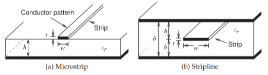
Figure \(\PageIndex{1}\): Planar transmission lines.