
3.1: Introduction
- Page ID
- 41025

\( \newcommand{\vecs}[1]{\overset { \scriptstyle \rightharpoonup} {\mathbf{#1}} } \)
\( \newcommand{\vecd}[1]{\overset{-\!-\!\rightharpoonup}{\vphantom{a}\smash {#1}}} \)
\( \newcommand{\id}{\mathrm{id}}\) \( \newcommand{\Span}{\mathrm{span}}\)
( \newcommand{\kernel}{\mathrm{null}\,}\) \( \newcommand{\range}{\mathrm{range}\,}\)
\( \newcommand{\RealPart}{\mathrm{Re}}\) \( \newcommand{\ImaginaryPart}{\mathrm{Im}}\)
\( \newcommand{\Argument}{\mathrm{Arg}}\) \( \newcommand{\norm}[1]{\| #1 \|}\)
\( \newcommand{\inner}[2]{\langle #1, #2 \rangle}\)
\( \newcommand{\Span}{\mathrm{span}}\)
\( \newcommand{\id}{\mathrm{id}}\)
\( \newcommand{\Span}{\mathrm{span}}\)
\( \newcommand{\kernel}{\mathrm{null}\,}\)
\( \newcommand{\range}{\mathrm{range}\,}\)
\( \newcommand{\RealPart}{\mathrm{Re}}\)
\( \newcommand{\ImaginaryPart}{\mathrm{Im}}\)
\( \newcommand{\Argument}{\mathrm{Arg}}\)
\( \newcommand{\norm}[1]{\| #1 \|}\)
\( \newcommand{\inner}[2]{\langle #1, #2 \rangle}\)
\( \newcommand{\Span}{\mathrm{span}}\) \( \newcommand{\AA}{\unicode[.8,0]{x212B}}\)
\( \newcommand{\vectorA}[1]{\vec{#1}} % arrow\)
\( \newcommand{\vectorAt}[1]{\vec{\text{#1}}} % arrow\)
\( \newcommand{\vectorB}[1]{\overset { \scriptstyle \rightharpoonup} {\mathbf{#1}} } \)
\( \newcommand{\vectorC}[1]{\textbf{#1}} \)
\( \newcommand{\vectorD}[1]{\overrightarrow{#1}} \)
\( \newcommand{\vectorDt}[1]{\overrightarrow{\text{#1}}} \)
\( \newcommand{\vectE}[1]{\overset{-\!-\!\rightharpoonup}{\vphantom{a}\smash{\mathbf {#1}}}} \)
\( \newcommand{\vecs}[1]{\overset { \scriptstyle \rightharpoonup} {\mathbf{#1}} } \)
\( \newcommand{\vecd}[1]{\overset{-\!-\!\rightharpoonup}{\vphantom{a}\smash {#1}}} \)
\(\newcommand{\avec}{\mathbf a}\) \(\newcommand{\bvec}{\mathbf b}\) \(\newcommand{\cvec}{\mathbf c}\) \(\newcommand{\dvec}{\mathbf d}\) \(\newcommand{\dtil}{\widetilde{\mathbf d}}\) \(\newcommand{\evec}{\mathbf e}\) \(\newcommand{\fvec}{\mathbf f}\) \(\newcommand{\nvec}{\mathbf n}\) \(\newcommand{\pvec}{\mathbf p}\) \(\newcommand{\qvec}{\mathbf q}\) \(\newcommand{\svec}{\mathbf s}\) \(\newcommand{\tvec}{\mathbf t}\) \(\newcommand{\uvec}{\mathbf u}\) \(\newcommand{\vvec}{\mathbf v}\) \(\newcommand{\wvec}{\mathbf w}\) \(\newcommand{\xvec}{\mathbf x}\) \(\newcommand{\yvec}{\mathbf y}\) \(\newcommand{\zvec}{\mathbf z}\) \(\newcommand{\rvec}{\mathbf r}\) \(\newcommand{\mvec}{\mathbf m}\) \(\newcommand{\zerovec}{\mathbf 0}\) \(\newcommand{\onevec}{\mathbf 1}\) \(\newcommand{\real}{\mathbb R}\) \(\newcommand{\twovec}[2]{\left[\begin{array}{r}#1 \\ #2 \end{array}\right]}\) \(\newcommand{\ctwovec}[2]{\left[\begin{array}{c}#1 \\ #2 \end{array}\right]}\) \(\newcommand{\threevec}[3]{\left[\begin{array}{r}#1 \\ #2 \\ #3 \end{array}\right]}\) \(\newcommand{\cthreevec}[3]{\left[\begin{array}{c}#1 \\ #2 \\ #3 \end{array}\right]}\) \(\newcommand{\fourvec}[4]{\left[\begin{array}{r}#1 \\ #2 \\ #3 \\ #4 \end{array}\right]}\) \(\newcommand{\cfourvec}[4]{\left[\begin{array}{c}#1 \\ #2 \\ #3 \\ #4 \end{array}\right]}\) \(\newcommand{\fivevec}[5]{\left[\begin{array}{r}#1 \\ #2 \\ #3 \\ #4 \\ #5 \\ \end{array}\right]}\) \(\newcommand{\cfivevec}[5]{\left[\begin{array}{c}#1 \\ #2 \\ #3 \\ #4 \\ #5 \\ \end{array}\right]}\) \(\newcommand{\mattwo}[4]{\left[\begin{array}{rr}#1 \amp #2 \\ #3 \amp #4 \\ \end{array}\right]}\) \(\newcommand{\laspan}[1]{\text{Span}\{#1\}}\) \(\newcommand{\bcal}{\cal B}\) \(\newcommand{\ccal}{\cal C}\) \(\newcommand{\scal}{\cal S}\) \(\newcommand{\wcal}{\cal W}\) \(\newcommand{\ecal}{\cal E}\) \(\newcommand{\coords}[2]{\left\{#1\right\}_{#2}}\) \(\newcommand{\gray}[1]{\color{gray}{#1}}\) \(\newcommand{\lgray}[1]{\color{lightgray}{#1}}\) \(\newcommand{\rank}{\operatorname{rank}}\) \(\newcommand{\row}{\text{Row}}\) \(\newcommand{\col}{\text{Col}}\) \(\renewcommand{\row}{\text{Row}}\) \(\newcommand{\nul}{\text{Nul}}\) \(\newcommand{\var}{\text{Var}}\) \(\newcommand{\corr}{\text{corr}}\) \(\newcommand{\len}[1]{\left|#1\right|}\) \(\newcommand{\bbar}{\overline{\bvec}}\) \(\newcommand{\bhat}{\widehat{\bvec}}\) \(\newcommand{\bperp}{\bvec^\perp}\) \(\newcommand{\xhat}{\widehat{\xvec}}\) \(\newcommand{\vhat}{\widehat{\vvec}}\) \(\newcommand{\uhat}{\widehat{\uvec}}\) \(\newcommand{\what}{\widehat{\wvec}}\) \(\newcommand{\Sighat}{\widehat{\Sigma}}\) \(\newcommand{\lt}{<}\) \(\newcommand{\gt}{>}\) \(\newcommand{\amp}{&}\) \(\definecolor{fillinmathshade}{gray}{0.9}\)The majority of transmission lines used in high-speed digital, RF, and microwave circuits are planar, as these can be defined using masks, photoresist, and etching of metal sheets. The most common planar transmission line is the microstrip line shown in Figure \(\PageIndex{1}\) and in cross section in Figure \(\PageIndex{2}\). This cross section is typical of what would be found on a semiconductor or printed wiring board (PWB), which is also called a printed circuit board (PCB). Current flows in both the top and bottom conductor, but in opposite directions. The physics is such that if there is a signal current on the top conductor, there must be a return signal current, which will tend to be as close to the signal current as possible to minimize stored energy. The provision of a signal return path close to the signal path is important in maintaining the integrity of (i.e., a predictable signal waveform on) an interconnect.
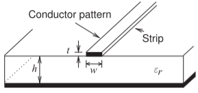
Figure \(\PageIndex{1}\): Microstrip transmission line.
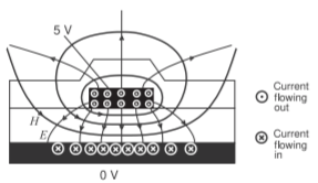
Figure \(\PageIndex{2}\): Cross-sectional view of a microstrip line showing electric and magnetic field lines and current flow. The electric and magnetic fields are in two mediums—the dielectric and air. If the line is homogeneous (the same dielectric everywhere) the electric and magnetic fields are only in the transverse plane, a field configuration known as the transverse electromagnetic mode (TEM).
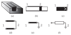
Figure \(\PageIndex{3}\): Representations of a shorted microstrip line with a short (or via) at port 2: (a) three-dimensional (3D) view indicating via; (b) side view; (c) top view with via indicated by \(\mathsf{X}\); (d) schematic representation of transmission line; (e) alternative schematic representation; and (f) representation as a circuit element.
In the microstrip line, electric field lines start on one of the conductors and finish on the other and are located almost entirely in the plane transverse to the long length of the line. The magnetic field is also mostly confined to the transverse plane, and so this line is referred to as a transverse electromagnetic (TEM) line. Integrating the electric field along a path gives the voltage. Since the voltage between the top and bottom conductors is more or less the same everywhere, longer \(E\) field lines correspond to lower levels of \(E\) field. The strength of the \(E\) field is also indicated by the density of the \(E\) field lines. This is a drawing convention for both electric and magnetic fields. A further comment is warranted for this line. This line is more accurately called a quasi-TEM line, as the longitudinal fields, particularly in the air region, are not negligible. The relative level of the longitudinal fields increases with frequency, but below about \(10\text{ GHz}\) and for typical dimensions used, the line is still essentially TEM. In Figure \(\PageIndex{2}\) current flows in the strip and a return current flows in what is normally regarded as the ground conductor. Both the signal and return currents induce a magnetic field and the closed path integral of the magnetic field is equal to the current enclosed by the path.
Various schematic representations of a microstrip line are used. Consider the representations in Figure \(\PageIndex{3}\) of a length of microstrip line shorted by a via at the end denoted by “2” (specifically the “2” refers to Port 2). The views in Figure \(\PageIndex{3}\)(a and b) provide perspectives. The representations shown in Figure \(\PageIndex{3}\)(d–f) are symbols used in circuit diagrams with the one used depending on the number of microstrip lines in a circuit diagram. If a circuit diagram has many transmission line elements, then the simple representation of Figure \(\PageIndex{3}\)(f) is most common. If there are few transmission line elements, then the representation of Figure \(\PageIndex{3}\)(d) is most common.