
3.8: Co-Planar Waveguide
- Page ID
- 41034

Microstrip is the most popular medium for circuit design at frequencies ranging from several hundred megahertz to tens of gigahertz. However, the electrical characteristics of a microstrip line are sensitive to variations of substrate thickness, and radiation from a microstrip line increases when the substrate is thick. The substrate thickness is not well controlled and can vary by \(1\%–5\%\) in many substrate technologies. As a result, the characteristic impedance will change by about the same amount. This is not acceptable in many designs where it is desirable that microstrip synthesis be accurate to \(1\%\) or so. The lateral dimensions, however, are well controlled being photolithographically defined and then etched.
A solution to the problems of microstrip is coplanar waveguide (CPW) shown in Figure \(\PageIndex{1}\)(a). CPW consists of a central strip flanked by two metal half-planes that carry the return current. The outer conductors can be regarded as ground, but they do not need to be explicitly connected to ground. Provided that the substrate is sufficiently thick, in practice this means that the substrate thickness is two or three times greater than both the strip width \(w\) and the metal separation \(s\), the electrical characteristics of CPW are entirely determined by the lateral dimensions, since all of the metallization is on one layer.
Of course, the infinite half-grounds of CPW cannot be produced so a more realistic implementation of CPW is finite ground CPW (FGCPW), shown in Figure \(\PageIndex{1}\)(b), where the signal return conductors are of finite width. For both the CPW and FGCPW lines, the vitalization and currents
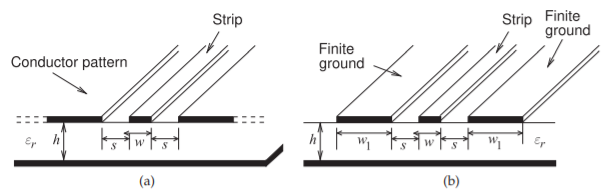
Figure \(\PageIndex{1}\): Coplanar waveguide (CPW): (a) conventional; and (b) finite ground CPW (FGCPW).
are confined to a single layer. However, the following discussion focuses on the idealized CPW structure in Figure \(\PageIndex{1}\)(a) as this has been studied extensively. However, the characteristics of FGCPW are very close to those of CPW if \(w_{1} ≥ 3w\) (see Figure \(\PageIndex{1}\)(b)).
3.8.1 Effective Permittivity and Characteristic Impedance of CPW
The fields in CPW, and thus the EM energy, are almost equally divided between air and dielectric, especially when the gap is small relative to the thickness of the dielectric. The effective relative permittivity of CPW is [28]
\[\begin{align}\varepsilon_{e}=\varepsilon_{r,e}&=0.5(\varepsilon_{r} + 1) \{\tanh[1.785 \log(h/s)+1.75] \nonumber \\ \label{eq:1} &\quad +(ks/h)[0.04 − 0.7k + 0.01(1 − 0.1\varepsilon_{r})(0.25 + k)]\}\end{align} \]
which is accurate to \(1.5\%\) for \(h/s ≥ 1\). In Equation \(\eqref{eq:1}\)
\[\label{eq:2}k=\frac{w}{w+2s} \]
Simply taking the effective permittivity as \((\varepsilon_{r} + 1)/2\) is a good starting point in analysis and design.
The characteristic impedance of CPW is [29]
\[\label{eq:3}Z_{0}=\frac{30\pi}{\sqrt{\varepsilon_{e}}}\frac{K'(k)}{K(k)} \]
where
\[\label{eq:4}k'=\sqrt{(1-k^{2})}\quad\text{and}\quad K'(k)=K(k') \]
\(K(k)\) and \(K(k′)\) are elliptic integrals, but the ratio, which is all that is required, is much simpler [30]:
\[\begin{align}\frac{K(k)}{K'(k)}&\approx\frac{1}{\pi}\ln\left(2\frac{1+\sqrt{k}}{1-\sqrt{k}}\right) &0\leq k\leq 0.707\nonumber \\ \label{eq:5} \\ \frac{K'(k)}{K(k)}&\approx\frac{1}{\pi}\ln\left(2\frac{1+\sqrt{k'}}{1-\sqrt{k'}}\right) &0.707<k\leq 1\end{align} \nonumber \]
Note that with CPW, \(Z_{0}\) is determined by the ratio of the center strip width \(w\) to the gap width \(s\). This makes the design of a CPW line with a particular \(Z_{0}\) non unique because an infinite range of \(w\) and \(s\) values will result in a specific \(Z_{0}\) requirement. This provides additional design flexibility.
A CPW line is fabricated on a \(500\:\mu\text{m}\) thick GaAs substrate, has a strip with a width of \(200\:\mu\text{m}\), and a gap of \(200\:\mu\text{m}\) between the strip and the ground planes. The relative permittivity of the substrate is \(12.85\) and the strip is \(10\:\mu\text{m}\) thick. What is the effective permittivity and characteristic impedance of the CPW line?
Solution
The structure is that shown in Figure \(\PageIndex{1}\)(a) with \(w = 500\:\mu\text{m},\: s = 200\:\mu\text{m},\: h = 500\:\mu\text{m}\), and \(t = 10\:\mu\text{m}\). From Equation \(\eqref{eq:2}\),
\[\label{eq:6}k=\frac{w}{w+2s}=\frac{500}{500+400}=0.556 \]
From Equation \(\eqref{eq:1}\),
\[\begin{align}\varepsilon_{e}&=0.5(12.85 + 1) \{\tanh[1.785 \log(500/200) + 1.75]\nonumber \\ &\quad +(0.556\cdot 200/500)[0.04 − 0.7\cdot 0.556 + 0.01(1 − 0.1\cdot 12.85)(0.25 + 0.556)]\} \nonumber \\ \label{eq:7}&=6.28\end{align} \]
This compares to \(\varepsilon_{e} = 6.925\) if the permittivities of air and the substrate are averaged.
Several quantities need to be calculated before calculating \(Z_{0}\). Since \(0 ≤ k ≤ 0.707\),
\[\label{eq:8}\frac{K(k)}{K'(k)}=\frac{1}{\pi}\ln\left(2\frac{1+\sqrt{k}}{1-\sqrt{k}}\right)=0.833 \]
Thus from Equation \(\eqref{eq:3}\),
\[\label{eq:9}Z_{0}=\frac{30\pi}{\sqrt{\varepsilon_{e}}}\frac{K'(k)}{K(k)}=45.1\:\Omega \]
3.8.2 Loss of CPW lines
Loss of a CPW line is primarily due to dielectric, radiative, and conductor losses. Dielectric loss is lower in a CPW line than in a microstrip line as the electric field lines are evenly divided between the air and dielectric, whereas with a microstrip line most of the field is concentrated in the dielectric. Also, radiation loss with CPW is much lower than with microstrip as the fields lines with a CPW line are much more tightly confined. In practice, when \(s/h\) is near to or greater than 1 the structure partially turns into a microstrip transmission line and it is of no use as a CPW line. This transfer of energy into the microstrip mode is another form of loss but can be avoided.
At low frequencies the strip resistance is
\[\label{eq:10}R_{\text{strip}}=R_{s}/w \]
where \(R_{s}\) is the sheet resistance of the strip and \(w\) is the width of the central strip. The ground resistance can be ignored as the ground current spreads out considerably and the resistances of each ground are in parallel, thus further reducing the ground resistance.
Approximately, the dielectric and conductive components of the attenuation are (if \(\omega,\:\mu_{0},\) and \(\varepsilon_{0}\) have SI units) [19]
\[\label{eq:11}\alpha_{D}=\frac{1}{2}\omega\sqrt{\mu_{0}\varepsilon_{0}\varepsilon_{r}}\tan\delta\text{ Np/m}\quad\text{and}\quad\alpha_{C}=\frac{R_{\text{strip}}}{2Z_{0}}\text{ Np/m} \]
respectively. So \(\alpha_{D}\) is almost entirely due to the choice of substrate material.
In summary, it is necessary to calculate the loss of CPW lines using EM simulation software to obtain the required accuracy. This is due to the more tightly confined fields and the greater variation of current densities compared to microstrip and stripline. A key attribute of CPW is the relative frequency independence of the effective permittivity, as this leads to almost dispersion-free transmission of signals. Also, devices can be connected along the signal path without using vias.
3.8.3 CPW Structures
The various CPW structures shown in Figure \(\PageIndex{2}\) are used to realize transmission line elements. The CPW-to-microstrip transition shown in
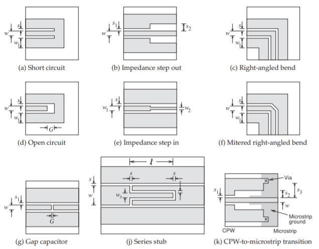
Figure \(\PageIndex{2}\): CPW structures.
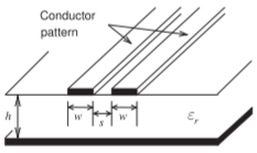
Figure \(\PageIndex{3}\): Differential line or coplanar strips (CPS).
Figure \(\PageIndex{2}\)(k) requires vias to transfer the ground plane from the same surface as the strip in the CPW line to the second metal plane that forms the ground of microstrip.
3.8.4 Differential Line and Coplanar Strip
A coplanar strip (CPS) line is shown in Figure \(\PageIndex{3}\). CPS has only two conductors separated by a narrow longitudinal slot. It is a balanced line structure and is occasionally implemented in applications including radiating elements and transitions. CPS has become important for on-chip implementations, especially for RFICs and high-speed digital signal transmission, where it is usually referred to as differential line.
CPS is closely related to CPW, as the signal return path is well defined and the electrical characteristics are independent of substrate thickness. CPS is a good structure to use instead of CPW when space is at a premium. Differential line is commonly used with RFICs, as the signal path on the IC is almost always differential since differential circuits on-chip remove many of the distortion and noise-coupling concerns. CPS suffers from relatively high radiation losses when realized on low-permittivity substrates. The radiation also results in substantial interaction and cross talk between adjacent circuits, although this is lower than with a microstrip line.
3.8.5 Summary
Coplanar waveguide is the transmission medium of choice above \(20\text{ GHz}\) or so, although the threshold for the switch from microstrip to CPW is higher for on-chip lines. CPW confines the EM fields in a more localized manner than does microstrip, thus reducing spurious coupling, radiation, and dispersion. The electrical characteristics of CPW are defined by the lateral dimensions that can be accurately defined photolithographically. This is a significant advantage when the thickness of a substrate cannot be accurately controlled. CPW provides a precisely defined signal return path and this reduces capacitive coupling of signal lines. CPS lines are also used as digital interconnect mediums where the desirable attribute is the differential signaling. Differential lines, having the same structure as CPS, are commonly used as off-chip transmission lines connecting RFICs.