
6.4: Rectangular Waveguide
- Page ID
- 41066

\( \newcommand{\vecs}[1]{\overset { \scriptstyle \rightharpoonup} {\mathbf{#1}} } \)
\( \newcommand{\vecd}[1]{\overset{-\!-\!\rightharpoonup}{\vphantom{a}\smash {#1}}} \)
\( \newcommand{\id}{\mathrm{id}}\) \( \newcommand{\Span}{\mathrm{span}}\)
( \newcommand{\kernel}{\mathrm{null}\,}\) \( \newcommand{\range}{\mathrm{range}\,}\)
\( \newcommand{\RealPart}{\mathrm{Re}}\) \( \newcommand{\ImaginaryPart}{\mathrm{Im}}\)
\( \newcommand{\Argument}{\mathrm{Arg}}\) \( \newcommand{\norm}[1]{\| #1 \|}\)
\( \newcommand{\inner}[2]{\langle #1, #2 \rangle}\)
\( \newcommand{\Span}{\mathrm{span}}\)
\( \newcommand{\id}{\mathrm{id}}\)
\( \newcommand{\Span}{\mathrm{span}}\)
\( \newcommand{\kernel}{\mathrm{null}\,}\)
\( \newcommand{\range}{\mathrm{range}\,}\)
\( \newcommand{\RealPart}{\mathrm{Re}}\)
\( \newcommand{\ImaginaryPart}{\mathrm{Im}}\)
\( \newcommand{\Argument}{\mathrm{Arg}}\)
\( \newcommand{\norm}[1]{\| #1 \|}\)
\( \newcommand{\inner}[2]{\langle #1, #2 \rangle}\)
\( \newcommand{\Span}{\mathrm{span}}\) \( \newcommand{\AA}{\unicode[.8,0]{x212B}}\)
\( \newcommand{\vectorA}[1]{\vec{#1}} % arrow\)
\( \newcommand{\vectorAt}[1]{\vec{\text{#1}}} % arrow\)
\( \newcommand{\vectorB}[1]{\overset { \scriptstyle \rightharpoonup} {\mathbf{#1}} } \)
\( \newcommand{\vectorC}[1]{\textbf{#1}} \)
\( \newcommand{\vectorD}[1]{\overrightarrow{#1}} \)
\( \newcommand{\vectorDt}[1]{\overrightarrow{\text{#1}}} \)
\( \newcommand{\vectE}[1]{\overset{-\!-\!\rightharpoonup}{\vphantom{a}\smash{\mathbf {#1}}}} \)
\( \newcommand{\vecs}[1]{\overset { \scriptstyle \rightharpoonup} {\mathbf{#1}} } \)
\( \newcommand{\vecd}[1]{\overset{-\!-\!\rightharpoonup}{\vphantom{a}\smash {#1}}} \)
\(\newcommand{\avec}{\mathbf a}\) \(\newcommand{\bvec}{\mathbf b}\) \(\newcommand{\cvec}{\mathbf c}\) \(\newcommand{\dvec}{\mathbf d}\) \(\newcommand{\dtil}{\widetilde{\mathbf d}}\) \(\newcommand{\evec}{\mathbf e}\) \(\newcommand{\fvec}{\mathbf f}\) \(\newcommand{\nvec}{\mathbf n}\) \(\newcommand{\pvec}{\mathbf p}\) \(\newcommand{\qvec}{\mathbf q}\) \(\newcommand{\svec}{\mathbf s}\) \(\newcommand{\tvec}{\mathbf t}\) \(\newcommand{\uvec}{\mathbf u}\) \(\newcommand{\vvec}{\mathbf v}\) \(\newcommand{\wvec}{\mathbf w}\) \(\newcommand{\xvec}{\mathbf x}\) \(\newcommand{\yvec}{\mathbf y}\) \(\newcommand{\zvec}{\mathbf z}\) \(\newcommand{\rvec}{\mathbf r}\) \(\newcommand{\mvec}{\mathbf m}\) \(\newcommand{\zerovec}{\mathbf 0}\) \(\newcommand{\onevec}{\mathbf 1}\) \(\newcommand{\real}{\mathbb R}\) \(\newcommand{\twovec}[2]{\left[\begin{array}{r}#1 \\ #2 \end{array}\right]}\) \(\newcommand{\ctwovec}[2]{\left[\begin{array}{c}#1 \\ #2 \end{array}\right]}\) \(\newcommand{\threevec}[3]{\left[\begin{array}{r}#1 \\ #2 \\ #3 \end{array}\right]}\) \(\newcommand{\cthreevec}[3]{\left[\begin{array}{c}#1 \\ #2 \\ #3 \end{array}\right]}\) \(\newcommand{\fourvec}[4]{\left[\begin{array}{r}#1 \\ #2 \\ #3 \\ #4 \end{array}\right]}\) \(\newcommand{\cfourvec}[4]{\left[\begin{array}{c}#1 \\ #2 \\ #3 \\ #4 \end{array}\right]}\) \(\newcommand{\fivevec}[5]{\left[\begin{array}{r}#1 \\ #2 \\ #3 \\ #4 \\ #5 \\ \end{array}\right]}\) \(\newcommand{\cfivevec}[5]{\left[\begin{array}{c}#1 \\ #2 \\ #3 \\ #4 \\ #5 \\ \end{array}\right]}\) \(\newcommand{\mattwo}[4]{\left[\begin{array}{rr}#1 \amp #2 \\ #3 \amp #4 \\ \end{array}\right]}\) \(\newcommand{\laspan}[1]{\text{Span}\{#1\}}\) \(\newcommand{\bcal}{\cal B}\) \(\newcommand{\ccal}{\cal C}\) \(\newcommand{\scal}{\cal S}\) \(\newcommand{\wcal}{\cal W}\) \(\newcommand{\ecal}{\cal E}\) \(\newcommand{\coords}[2]{\left\{#1\right\}_{#2}}\) \(\newcommand{\gray}[1]{\color{gray}{#1}}\) \(\newcommand{\lgray}[1]{\color{lightgray}{#1}}\) \(\newcommand{\rank}{\operatorname{rank}}\) \(\newcommand{\row}{\text{Row}}\) \(\newcommand{\col}{\text{Col}}\) \(\renewcommand{\row}{\text{Row}}\) \(\newcommand{\nul}{\text{Nul}}\) \(\newcommand{\var}{\text{Var}}\) \(\newcommand{\corr}{\text{corr}}\) \(\newcommand{\len}[1]{\left|#1\right|}\) \(\newcommand{\bbar}{\overline{\bvec}}\) \(\newcommand{\bhat}{\widehat{\bvec}}\) \(\newcommand{\bperp}{\bvec^\perp}\) \(\newcommand{\xhat}{\widehat{\xvec}}\) \(\newcommand{\vhat}{\widehat{\vvec}}\) \(\newcommand{\uhat}{\widehat{\uvec}}\) \(\newcommand{\what}{\widehat{\wvec}}\) \(\newcommand{\Sighat}{\widehat{\Sigma}}\) \(\newcommand{\lt}{<}\) \(\newcommand{\gt}{>}\) \(\newcommand{\amp}{&}\) \(\definecolor{fillinmathshade}{gray}{0.9}\)A rectangular waveguide is shown in Figure \(\PageIndex{1}\)(a). Rectangular waveguides guide EM energy between four connected electrical walls, and there is little current created on the walls. As a result, resistive losses are quite low, much lower than can be achieved using coaxial lines for example. One of the major uses of a rectangular waveguide is when losses must be kept to a minimum, so that a rectangular waveguide is used in very high-power situations such as radar, and at a few tens of gigahertz and above. At higher frequencies the loss of coaxial lines becomes very large, and it also becomes difficult to build small-diameter coaxial lines at \(100\text{ GHz}\) and above. As a result, a rectangular waveguide is nearly always used above \(100\text{ GHz}\). There are many low- to medium-power legacy systems that use rectangular waveguides down to \(1\text{ GHz}\).
A rectangular waveguide supports many different modes, but it does not support the TEM mode. The modes are categorized as being either TM or TE, denoting whether all of the magnetic fields are perpendicular to the direction of propagation (these are the transverse magnetic fields) or whether all of the electric fields are perpendicular to the direction of propagation (these are the transverse electric fields). Dimensions of the waveguide can be chosen so that only one mode can propagate for a range of frequencies. With more than one mode propagating, the different components of a signal would travel at different speeds and thus combine at a load incoherently, since the ratio of the energy in the modes would vary (usually) randomly.
The TE and TM field descriptions are derived from the solution of differential equations—Maxwell’s equations—subject to boundary conditions. The general solutions for rectangular systems are sinewaves and there are possibly many discrete solutions. The nomenclature that has developed over
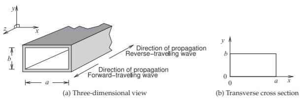
Figure \(\PageIndex{1}\): Rectangular waveguide with internal dimensions of \(a\) and \(b\).
the years to classify modes references the number of variations in the \(x\) direction, using the index \(m\), and the number of variations in the \(y\) direction, using the index \(n\). So there are \(\text{TE}_{mn}\) and \(\text{TM}_{mn}\) modes, and dimensions are usually selected so that only the \(TE_{10}\) mode can propagate.
6.4.1 TM Modes
The development of the field descriptions for the TM modes begins with the rectangular wave equations derived in Section 6.2. Transverse magnetic waves have zero \(H_{z}\), but nonzero \(E_{z}\). The differential equation governing \(E_{z}\) is, in rectangular coordinates (from Equations (6.2.13) and (6.2.16)),
\[\label{eq:1}\nabla_{t}^{2}E_{z}=\frac{\partial^{2}E_{z}}{\partial x^{2}}+\frac{\partial^{2}E_{z}}{\partial y^{2}}=-k_{c}^{2}E_{z} \]
Using a separation of variables procedure, this equation has the solution
\[\label{eq:2}E_{z} = [A′ \sin(k_{x}x) + B′ \cos(k_{x}x)] [C′ \sin(k_{y}y) + D′ \cos(k_{y}y)] \text{e}^{−\gamma z} \]
where
\[\label{eq:3}k_{x}^{2}+k_{y}^{2}=k_{c}^{2} \]
The perfectly conducting boundary at \(x = 0\) requires \(B′ = 0\) to produce \(E_{z} = 0\) there. Similarly the ideal boundary at \(y = 0\) requires \(D′ = 0\). Replacing \(A′ C′\) by a new constant \(A\), then
\[\label{eq:4}E_{z} = A \sin(k_{x}x) \sin(k_{y}y)\text{e}^{−\gamma z} \]
The axial electric field, \(E_{z}\), must also be zero at \(x = a\) and \(y = b\). This can only be so (except for the trivial solution \(A = 0\)) if \(k_{x}a\) is an integral multiple of \(\pi\) so that \(\sin(k_{x}a)=0\):
\[\label{eq:5}k_{x}a=m\pi,\quad m=1,2,3,\ldots \]
Similarly, for \(E_{z}\) to be zero at \(y = b\), \(\sin(k_{y}b)=0\) and \(k_{y}b\) must also be a multiple of \(\pi\):
\[\label{eq:6}k_{y}b=n\pi,\quad n=1,2,3,\ldots \]
So the cutoff frequency of the TM wave with \(m\) variations in \(x\) and with \(n\) variations in \(y\) (i.e., the \(\text{TM}_{mn}\) mode) is, from Equation \(\eqref{eq:3}\),
\[\label{eq:7}f_{c_{m,n}}=\frac{k_{c_{m,n}}}{2\pi\sqrt{\mu\varepsilon}}=\frac{1}{2\pi\sqrt{\mu\varepsilon}}\left[\left(\frac{m\pi}{a}\right)^{2}+\left(n\frac{\pi}{b}\right)^{2}\right]^{1/2} \]
The remaining field components of the \(\text{TM}_{mn}\) wave are found with \(H_{z} = 0\) and \(E_{z}\) from Equation \(\eqref{eq:4}\) and Equation (6.2.25)):
\[\begin{align}\label{eq:8}E_{x}&=-\frac{\gamma k_{x}}{k_{c_{m,n}}^{2}}A\cos(k_{x}x)\sin(k_{y}y)\text{e}^{-\gamma z} \\ \label{eq:9}E_{y}&=-\frac{\gamma k_{y}}{k_{c_{m,n}}^{2}}A\sin(k_{x}x)\cos(k_{y}y)\text{e}^{-\gamma z} \\ \label{eq:10}H_{x}&=\frac{\jmath\omega\varepsilon k_{y}}{k_{c_{m,n}}^{2}}A\sin(k_{x}x)\cos(k_{y}y)\text{e}^{-\gamma z} \\ \label{eq:11}H_{y}&=-\frac{\jmath\omega\varepsilon k_{x}}{k_{c_{m,n}}^{2}}A\cos(k_{x}x)\sin(k_{y}y)\text{e}^{-\gamma z}\end{align} \]
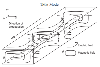
Figure \(\PageIndex{2}\): Electric and magnetic field distribution for the lowest-order TM mode, the \(\text{TM}_{11}\) mode.
The spatial field variations depend on the \(x\) and \(y\) cutoff wavenumbers, \(k_{x}\) and \(k_{y}\), which in turn depend on the mode indexes and the cross-sectional dimensions of the waveguide. The cutoff wavenumber, \(k_{c}\), is a function of the \(m\) and \(n\) indexes, and so \(k_{c_{m,n}}\) is often used for the cutoff wavenumber with
\[\label{eq:12}k_{c_{m,n}}^{2}=k_{x,m}^{2}+k_{y,n}^{2}=\left(\frac{m\pi}{a}\right)^{2}+\left(\frac{n\pi}{b}\right)^{2} \]
The lowest-order TM mode is the \(\text{TM}_{11}\) mode, with \(m = 1\) and \(n = 1\), and this has the minimum variation of the fields (of any TM mode); these are shown in Figure \(\PageIndex{2}\).
In summary, a mode can propagate only at frequencies above the cutoff frequency. Another quantity that defines when cutoff occurs is the cutoff wavelength, defined as
\[\label{eq:13}\lambda_{c}=\frac{\nu}{f_{c_{m,n}}} \]
where \(\nu = 1/\sqrt{\mu\varepsilon}\) is the velocity of a TEM mode in the medium (and of course this is not a rectangular waveguide mode). The cutoff wavelength is the wavelength in the medium (without the waveguide walls) at which cutoff occurs. Since \(k_{c}^{2}\) is \(k^{2} −\beta^{2}\), the attenuation constant of a given mode for frequencies below the cutoff frequency is
\[\label{eq:14}\alpha=\sqrt{k_{c_{m,n}}^{2}-k^{2}}=k_{c_{m,n}}\sqrt{1-\left(\frac{f}{f_{c_{m,n}}}\right)^{2}},\quad f<f_{c_{m,n}} \]
The phase constant for frequencies above the cutoff frequency is
\[\label{eq:15}\beta=\sqrt{k^{2}-k_{c_{m,n}}^{2}}=k\sqrt{1-\left(\frac{f_{c_{m,n}}}{f}\right)^{2}},\quad f>f_{c_{m,n}} \]
For a propagating mode (i.e., \(f>f_{c_{m,n}}\)) the wavelength of the mode, called the guide wavelength, is
\[\label{eq:16}\lambda_{g}=\frac{2\pi}{\beta}=\frac{\lambda}{\sqrt{1-(f_{c}/f)^{2}}} \]
where \(\lambda\) is the wavelength of a TEM mode in the medium (but of course not in the waveguide): \(\lambda = \nu/f\). The phase velocity of the mode is also dependent on the mode indexes \(m\) and \(n\) through the cutoff frequency,
\[\label{eq:17}v_{p}=\frac{\omega}{\beta}=\frac{\nu}{\sqrt{1-(f_{c_{m,n}}/f)^{2}}} \]
and the group velocity is
\[\label{eq:18}v_{g}=\frac{d\omega}{d\beta}=\nu\sqrt{1-(f_{c_{m,n}}/f)^{2}} \]
6.4.2 TE Modes
Transverse electric waves have zero \(E_{z}\) and nonzero \(H_{z}\) so that, in rectangular coordinates,
\[\label{eq:19}\nabla_{t}^{2}H_{z}=\frac{\partial^{2}H_{z}}{\partial x^{2}}+\frac{\partial^{2}H_{z}}{\partial y^{2}}=-k_{c}^{2}H_{z} \]
Solving using the separation of variables technique gives
\[\label{eq:20}H_{z} = [A′′ \sin(k_{x}x) + B′′ \cos(k_{x}x)] [C′′ \sin(k_{y}y) + D′′ \cos(k_{y}y)] \text{e}^{−\gamma z} \]
where
\[\label{eq:21}k_{x}^{2}+k_{y}^{2}=k_{c}^{2} \]
Imposition of a boundary condition in this case is a little less direct, but the electric field components are
\[\begin{align}\label{eq:22}E_{x}&=-\frac{\jmath\omega\mu}{k_{c}^{2}}\frac{\partial H_{z}}{\partial y} \\ &=-\frac{\jmath\omega\mu k_{y}}{k_{c}^{2}}[A′′ \sin(k_{x}x) + B′′ \cos(k_{x}x)] [C′′ \cos(k_{y}y) − D′′ \sin(k_{y}y)]\text{e}^{−\gamma z} \\ \label{eq:23}E_{y}&=\frac{\jmath\omega\mu}{k_{c}^{2}}\frac{\partial H_{z}}{\partial x} \\ &=\frac{\jmath\omega\mu k_{x}}{k_{c}^{2}}[A′′ \cos(k_{x}x) − B′′ \sin(k_{x}x)] [C′′ \sin(k_{y}y) + D′′ \cos(k_{y}y)] \text{e}^{−\gamma z}\end{align} \nonumber \]
For \(E_{x}\) to be zero at \(y = 0\) for all \(x\), \(C′′ = 0\); and for \(E_{y} = 0\) at \(x = 0\) for all \(y\), \(A′′ = 0\). Defining \(B′′D′′ = B\), then
\[\begin{align}\label{eq:24}H_{z} &= B \cos(k_{x}x) \cos(k_{y}y) \\ \label{eq:25}E_{x}&=\frac{\jmath\omega\mu k_{y}}{k_{c}^{2}}B\cos(k_{x}x)\sin(k_{y}y)\text{e}^{-\gamma z} \\ \label{eq:26}E_{y}&=-\frac{\jmath\omega\mu k_{x}}{k_{c}^{2}}B\sin(k_{x}x)\cos(k_{y}y)\text{e}^{-\gamma z}\end{align} \]
\(E_{y}\) is zero at \(x = a\), that is, \(\sin(k_{x}a)=0\), so that \(k_{x}a\) must be a multiple of \(\pi\):
\[\label{eq:27}k_{x}a=m\pi,\quad m=1,2,3,\ldots \]
Also, \(E_{x}\) is zero at \(y = b\), that is, \(\sin(k_{y}b)=0\), so that \(k_{y}b\) must be zero (so that \(E_{x}\) is always zero) or that it is a multiple of \(\pi\). Therefore
\[\label{eq:28}k_{y}b=n\pi\quad n=0,1,2,3,\ldots \]
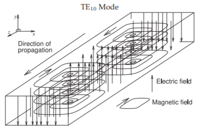
Figure \(\PageIndex{3}\): Electric and magnetic field distribution for the lowest-order TE mode.
The forms of the transverse electric field are then
\[\begin{align}\label{eq:29}E_{x}&=\frac{\jmath\omega\mu k_{y}}{k_{c_{m,n}}^{2}}B \cos(k_{x}x) \sin(k_{y}y)\text{e}^{−\gamma z} \\ \label{eq:30}E_{y}&=-\frac{\jmath\omega\mu k_{x}}{k_{c_{m,n}}^{2}}B \sin(k_{x}x) \cos(k_{y}y)\text{e}^{−\gamma z}\end{align} \]
and the corresponding transverse magnetic field components are
\[\begin{align}\label{eq:31}H_{x}&=\frac{\gamma k_{x}}{k_{c_{m,n}}^{2}}B \sin(k_{x}x) \cos(k_{y}y)\text{e}^{−\gamma z} \\ \label{eq:32} H_{y}&=\frac{\gamma k_{y}}{k_{c_{m,n}}^{2}}B \cos(k_{x}x) \sin(k_{y}y)\text{e}^{−\gamma z}\end{align} \]
Here the use of \(k_{c_{m,n}}\) emphasizes that the cutoff wavenumber is a function of the \(m\) and \(n\) indexes:
\[\label{eq:33}k_{c_{m,n}}^{2}=k_{x,m}^{2}+k_{y,n}^{2}=\left(\frac{m\pi}{a}\right)^{2}+\left(\frac{n\pi}{b}\right)^{2} \]
The lowest-order TE mode is the \(\text{TE}_{10}\) mode (with \(m = 1\) and \(n = 0\)) and this has the minimum variation of the fields; these are shown in Figure \(\PageIndex{3}\).
6.4.3 Practical Rectangular Waveguide
The dimensions and operating frequencies of a rectangular waveguide are chosen to support only one propagating mode. The operating frequency is between the cutoff frequency of the mode with the lowest cutoff frequency and the cutoff frequency of the mode with the next lowest cutoff frequency. Thus only one mode propagates.
Referring to Figure \(\PageIndex{1}\), if the dimensions are chosen so that \(b\) is greater than \(a\), then the lowest-order TE mode (the \(\text{TE}_{10}\) mode) has one variation of the fields in the \(x\) direction, while the lowest-order TM mode (the \(\text{TM}_{11}\) mode) has one variation of the field in the \(x\) direction and one variation in the \(y\) direction. Thus the cutoff frequency of the \(\text{TM}_{11}\) mode will be higher than the cutoff frequency of the \(\text{TE}_{10}\) mode. Below the cutoff frequency the modes will not propagate (i.e., \(\beta\) (the imaginary part of the propagation constant) is zero). The propagation constants of the rectangular waveguide
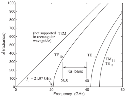
Figure \(\PageIndex{4}\): Dispersion diagram of waveguide modes in air-filled \(\text{Ka}\)-band rectangular waveguide with internal dimensions of \(0.280\times 0.140\text{ inches}\) \((7.112\text{ mm}\times 3.556\text{ mm})\). \(\text{Ka}\)-band waveguide is used between \(26.5\text{ GHz}\) and \(40\text{ GHz}\). Over this frequency range only the \(\text{TE}_{10}\) mode propagates.
| Mode | Cut-off frequency \((\text{GHz})\) |
|---|---|
| \(\text{TEM}\) | not supported |
| \(\text{TE}_{10}\) | \(21.07\text{ GHz}\) |
| \(\text{TE}_{01}\) | \(42.15\text{ GHz}\) |
| \(\text{TE}_{11}\) | \(47.13\text{ GHz}\) |
| \(\text{TM}_{10}\) | not supported |
| \(\text{TM}_{01}\) | not supported |
| \(\text{TM}_{11}\) | \(47.13\text{ GHz}\) |
Table \(\PageIndex{1}\): Cut-off frequencies of several modes in \(\text{Ka}\)-Band waveguide nominally used between \(26.5\text{ GHz}\) and \(40\text{ GHz}\).
modes with the lowest cutoff frequencies are shown in Figure \(\PageIndex{4}\) for a \(\text{Ka}\)-band waveguide having internal dimensions of \(a = 0.280\text{ inches}\) and \(b = 0.140\text{ inches}\). This figure is known as a dispersion diagram and is sometimes plotted as \(\beta\) versus \(k\). There are four modes supported below \(60\text{ GHz}\) and the line corresponding to the TEM mode is provided for reference, as the TEM mode is not supported in a rectangular waveguide.
Not all possible low-order modes can be supported in rectangular waveguide as the boundary conditions cannot be satisfied (see Table \(\PageIndex{1}\)). The cutoff frequency of the \(\text{TE}_{10}\) mode is \(21.07\text{ GHz}\) and the next lowest cutoff mode, the \(\text{TE}_{01}\) mode, has a cutoff frequency of \(42.15\text{ GHz}\). The mode has a cutoff frequency which is the frequency when the wavelength (in the medium, or free-space wavelength if the guide is air-filled) is twice the \(a\) dimension of the waveguide (see Figure \(\PageIndex{1}\)). The next higher-order mode appears when it is possible for a variation in the \(y\) direction. This occurs at a frequency corresponding to the \(b\) dimension being one-half wavelength in the medium. The \(\text{TE}_{11}\) mode and \(\text{TM}_{11}\) modes have the same cutoff frequency of \(47.13\text{ GHz}\). In determining the operating frequency range both the phase and group velocity variations are considered. These are shown in Figure \(\PageIndex{5}\) for the \(\text{TE}_{10}\) mode, where they are normalized to \(c\) as the waveguide is air-filled. The group velocity, \(v_{g}\), varies substantially, especially near the cutoff frequency of the mode. As a result, the lower operating frequency of the mode is chosen to be substantially above the cutoff frequency. The upper limit of the operating frequency is chosen to be about \(5\%\) below the cutoff frequency of the second propagating mode. This
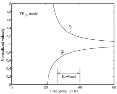
Figure \(\PageIndex{5}\): Normalized phase and group velocities of the \(\text{TE}_{10}\) mode in air-filled \(\text{Ka}\)-band waveguide.
is because small discontinuities can launch the higher-order mode. Thus the operating frequency of a \(\text{Ka}\)-band waveguide is \(26.5\text{ GHz}–40\text{ GHz}\), providing a margin of \(5.4\text{ GHz}\) at the low end, and \(2.2\text{ GHz}\) margin at the high end. So approximately one-half octave of bandwidth is supported by a rectangular waveguide if the wide dimension is twice the height of the waveguide. Since a rectangular waveguide is useful over a relatively narrow frequency range, standard dimensions have been developed, as listed in Table \(\PageIndex{2}\). A waveguide is referred to by its waveguide standard number (its WR designation), however, the old letter designations of bands are commonly used.
At times it is necessary to have a rectangular waveguide that can be used over more than one-half octave of bandwidth. This is achieved by reducing the height, \(b\), of the waveguide, producing what is called a reduced-height waveguide. By reducing \(b\) to one-quarter of \(a\), an octave of bandwidth can be obtained [2, 3, 4].
6.4.4 Rectangular Waveguide Components
Rectangular waveguide components require considerable machining, but the equivalents of many of the components that are available in microstrip can be realized. Invariably the lowest-order TE mode is used. This is the \(\text{TE}_{10}\) mode, with the field configuration shown in Figure \(\PageIndex{3}\). The characteristic of this mode is that the \(\text{E}\)-field is transverse to the direction of propagation. Many components have particular orientations to the planes of the \(\text{E}\) and \(\text{H}\) fields. Consider the rectangular waveguide bends shown in Figure \(\PageIndex{6}\). The bend in Figure \(\PageIndex{6}\)(a) is called an \(\text{H}\)-plane bend, or \(\text{H}\)-bend, as the axis of the waveguide (which is in the direction of propagation) always remains parallel to the \(\text{H}\) field. With the \(\text{E}\)-plane bend, or \(\text{E}\)-bend, in Figure \(\PageIndex{6}\)(b), the axis of the waveguide remains parallel to the \(\text{E}\) field. The flat sections at the end of the waveguide sections are called flanges. The pins in the flanges are alignment pins that insert into holes in the opposite flange.
In building circuits using rectangular waveguides, it is frequently necessary to rotate and twist the waveguide so that sections can be joined. Bends enable this, but twists (as shown in Figure \(\PageIndex{7}\)) are also used.
| Band | EIA Waveguide Band | Operating Frequency (\(\text{GHz}\)) | Internal Dimensions (\(a\times b\), inches) | \(\text{TE}_{10}\) Cutoff \((\text{GHz})\) |
|---|---|---|---|---|
| WR–2300 | \(0.32–0.49\) | \(23.000\times 11.500\) | \(0.257\) | |
| WR–2100 | \(0.35–0.53\) | \(21.000\times 10.500\) | \(0.281\) | |
| WR–1800 | \(0.43–0.62\) | \(18.000\times 9.000\) | \(0.328\) | |
| WR–1500 | \(0.49–0.74\) | \(15.000\times 7.500\) | \(0.393\) | |
| WR–1150 | \(0.64–0.96\) | \(11.500\times 5.750\) | \(0.513\) | |
| WR–1000 | \(0.75–1.1\) | \(9.975\times 4.875\) | \(0.592\) | |
| WR–770 | \(0.96–1.5\) | \(7.700\times 3.385\) | \(0.766\) | |
| WR-650 | \(1.12–1.70\) | \(6.500\times 3.250\) | \(0.908\) | |
| \(\text{R}\) | WR-430 | \(1.70-2.60\) | \(4.300\times 2.150\) | \(1.37\) |
| \(\text{D}\) | WR-340 | \(2.20-3.30\) | \(3.400\times 1.700\) | \(1.74\) |
| \(\text{S}\) | WR-284 | \(2.60-3.95\) | \(2.840\times 1.340\) | \(2.08\) |
| \(\text{E}\) | WR-229 | \(3.30-4.90\) | \(2.290\times 1.150\) | \(2.58\) |
| \(\text{G}\) | WR-187 | \(3.95-5.85\) | \(1.872\times 0.872\) | \(3.15\) |
| \(\text{F}\) | WR-159 | \(4.90-7.05\) | \(1.590\times 0.795\) | \(3.71\) |
| \(\text{C}\) | WR-137 | \(5.85-8.20\) | \(1.372\times 0.622\) | \(4.30\) |
| \(\text{H}\) | WR-112 | \(7.05-10.00\) | \(1.122\times 0.497\) | \(5.26\) |
| \(\text{X}\) | WR-90 | \(8.2-12.4\) | \(0.900\times 0.400\) | \(6.56\) |
| \(\text{Ku}\) | WR-62 | \(12.4-18.0\) | \(0.622\times 0.311\) | \(9.49\) |
| \(\text{K}\) | WR-51 | \(15.0-22.0\) | \(0.510\times 0.255\) | \(11.6\) |
| \(\text{K}\) | WR-42 | \(18.0-26.5\) | \(0.420\times 0.170\) | \(14.1\) |
| \(\text{Ka}\) | WR-28 | \(26.5-40.0\) | \(0.280\times 0.140\) | \(21.1\) |
| \(\text{Q}\) | WR-22 | \(33-50\) | \(0.224\times 0.112\) | \(26.3\) |
| \(\text{U}\) | WR-19 | \(40-60\) | \(0.188\times 0.094\) | \(31.4\) |
| \(\text{V}\) | WR-15 | \(50-75\) | \(0.148\times 0.074\) | \(39.9\) |
| \(\text{E}\) | WR-12 | \(60-90\) | \(0.122\times 0.061\) | \(48.4\) |
| \(\text{W}\) | WR-10 | \(75-110\) | \(0.100\times 0.050\) | \(59.0\) |
| \(\text{F}\) | WR-8 | \(90-140\) | \(0.080\times 0.040\) | \(73.8\) |
| \(\text{D}\) | WR-6 | \(110-170\) | \(0.0650\times 0.0325\) | \(90.8\) |
| \(\text{G}\) | WR-5 | \(140-220\) | \(0.0510\times 0.0255\) | \(116\) |
| WR-4 | \(170–260\) | \(0.0430\times 0.0215\) | \(137\) | |
| WR-3 | \(220–325\) | \(0.0340\times 0.0170\) | \(174\) | |
| \(\text{Y}\) | WR-2 | \(325–500\) | \(0.0200\times 0.0100\) | \(295\) |
| WR-1.5 | \(500–750\) | \(0.0150\times 0.0075\) | \(393\) | |
| WR-1 | \(750–1100\) | \(0.0100\times 0.0050\) | \(590\) |
Table \(\PageIndex{2}\): Waveguide bands, operating frequencies, and internal dimensions. Waveguide dimensions specified in inches (use \(25.4\text{ mm/inch}\) to convert to millimeters). The number in the WR designation is the long internal dimension of the waveguide in hundreds of an inch. The \(\text{TE}_{10}\) mode cutoff frequency is when the long dimension is one-half wavelength long (the free-space wavelength if vacuum- or air-filled, or modified by the square root of the permittivity if the waveguide is dielectric filled).
Waveguide tees are used to split and combine signals. There are both \(\text{E}\)-plane and \(\text{H}\)-plane versions, as there were for bends (see Figure \(\PageIndex{8}\)).
There is a wide variety of waveguide components. The components are developed from EM field considerations and not derived from current and voltage circuits. For example, a termination in a rectangular waveguide is realized using a resistive wedge of material as shown in Figure \(\PageIndex{9}\)(a). This provides a termination with a lower reactive component than would be obtained with a lumped resistor placed at the end of the line. The matched load absorbs all of the power in the traveling wave incident on it. The functional component is a lossy material, often shaped as a wedge or tall pyramid, that absorbs power over a distance corresponding, perhaps, to one-half wavelength or longer. So while the characteristic impedance of a wave in the rectangular waveguide varies with frequency, the termination is always matched to this impedance. A high-power waveguide matched load is shown in Figure \(\PageIndex{9}\)(b). This component uses the structure illustrated in Figure \(\PageIndex{9}\)(a) and has fins for the dissipation of heat. A waveguide
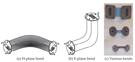
Figure \(\PageIndex{6}\): Rectangular waveguide bends. In (c), top is \(\text{X}\)-band (\(8–12\text{ GHz}\)), middle is \(\text{Ku}\)-band (\(12–18\text{ GHz}\)), and bottom is \(\text{Ka}\)-band (\(26–40\text{ GHz}\)).
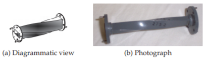
Figure \(\PageIndex{7}\): Rectangular waveguide twist.
attenuator is realized by introducing resistive material, as shown in Figure \(\PageIndex{9}\)(c). This introduces a section of line with a high attenuation coefficient. By controlling the depth of the resistive vane, as shown in Figure \(\PageIndex{9}\)(d), a variable attenuator is obtained.
Discontinuities in the waveguide introduce inductive, capacitive, and resonant elements. Several discontinuities that are used to realize these elements are shown in Figure \(\PageIndex{10}\). These illustrate most clearly the use of \(\text{E}\) and \(\text{H}\) field disturbances to realize capacitive and inductive components. An \(\text{E}\)-plane discontinuity (Figure \(\PageIndex{10}\)(a)) is modeled approximately by a frequency-dependent capacitor. \(\text{H}\)-plane discontinuities (Figure \(\PageIndex{10}\)(b and c)) resemble inductors, as does the circular iris of Figure \(\PageIndex{10}\)(d). The resonant waveguide iris of Figure \(\PageIndex{10}\)(e) disturbs the \(\text{E}\) and \(\text{H}\) fields and is modeled by a parallel \(LC\) resonant circuit near the frequency of resonance. Posts in the waveguide are used as reactive elements (Figure \(\PageIndex{10}\)(f)) and to mount active devices (Figure \(\PageIndex{10}\)(g)). The equivalent circuits of waveguide discontinuities are modeled by capacitive elements if the \(\text{E}\) field is interrupted and by inductive elements if the \(\text{H}\) field (or current) is disturbed. Many papers (e.g., [5, 6, 7, 8]) have been devoted to analytic field solutions that lead to equivalent lumped element representations of waveguide discontinuities that can then be used in synthesis.
A rectangular waveguide circulator is shown in Figure \(\PageIndex{11}\). A circulator uses a special property of magnetized ferrites that provides a preferred direction of EM propagation.
It is sometimes necessary to interface between waveguide series, and one component to do this is the tapered waveguide section shown in Figure \(\PageIndex{12}\)(a). Alternatively the one-quarter wavelength long impedance transformer
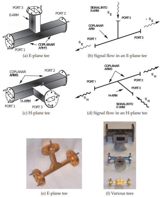
Figure \(\PageIndex{8}\): Rectangular waveguide tees: (a) three-dimensional representation of an \(\text{E}\)-plane tee; (b) description of the signal flow in an \(\text{E}\)-plane tee; (c) three-dimensional representation of an \(\text{H}\)-plane tee; (d) description of the signal flow in an \(\text{H}\)-plane tee; (e) photograph of an \(\text{E}\)-plane tee; and (f) photograph of waveguide tees for different waveguide bands (top, \(\text{X}\)-band \(\text{H}\)-plane tee; middle, \(\text{Ku}\)-band \(\text{H}\)-plane tee; bottom, \(\text{Ka}\)-band \(\text{E}\)-plane tee).
shown in Figure \(\PageIndex{12}\)(b) could be used. This section can be shorter than the tapered waveguide section, which, however, has higher bandwidth.
Other components commonly encountered are the waveguide switch (see Figure \(\PageIndex{12}\)(c)), the coaxial-to-waveguide adaptor (see Figure \(\PageIndex{13}\)), and the waveguide horn antenna (see Figure \(\PageIndex{12}\)(d)).
Distributed directional couplers are realized by two coupled transmission lines. A rectangular waveguide directional coupler is shown in Figure \(\PageIndex{14}\).
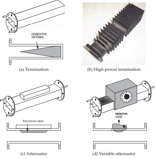
Figure \(\PageIndex{9}\): Terminations and attenuators in a rectangular waveguide.
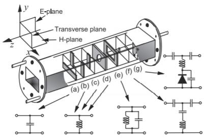
Figure \(\PageIndex{10}\): Rectangular waveguide discontinuities and their lumped equivalent circuits: (a) capacitive \(\text{E}\)-plane discontinuity; (b) inductive \(\text{H}\)-plane discontinuity; (c) symmetrical inductive \(\text{H}\)-plane discontinuity; (d) inductive post discontinuity; (e) resonant window discontinuity; (f) capacitive post discontinuity; and (g) diode post mount.
Here the two transmission lines, the rectangular waveguides, are coupled by slots in the common wall of the guides. In Figure \(\PageIndex{14}\)(b) the EM wave from the bottom waveguide leaks into the top waveguide through the coupling slots. A quick check on phasing indicates that the coupled wave in the reverse direction is canceled. Meanwhile, in the forward-traveling direction there is constructive interference of the coupled EM wave.
Variable elements available in a rectangular waveguide include the micrometer tuner, shown in Figure \(\PageIndex{15}\). The tuner shown in Figure \(\PageIndex{15}\)(a)
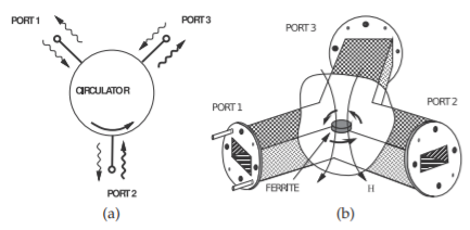
Figure \(\PageIndex{11}\): Waveguide circulator: (a) schematic; and (b) three-dimensional representation showing \(\text{H}\) field lines magnetizing a ferrite disk.
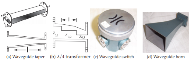
Figure \(\PageIndex{12}\): Waveguide components: (a) waveguide switch; (b) rectangular waveguide quarter-wavelength impedance transformer; (c) rectangular waveguide taper connecting one waveguide series to another; and (d) waveguide horn antenna.
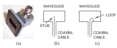
Figure \(\PageIndex{13}\): Coaxial transmission line to rectangular waveguide adaptor: (a) photograph; (b) adaptor using a coupling stub; and (c) adaptor using a coupling loop.
typically moves a reactive element along the waveguide. One example is the movable short circuit shown in Figure \(\PageIndex{5}\)(b). Another variable element used in tuning is the waveguide slide tuner, shown in Figure \(\PageIndex{15}\)(c). Here a slot is cut in the wide wall of the waveguide and a metal probe is inserted. The slot is in a region where the currents in the waveguide wall are minimum, so little discontinuity is introduced. The probe introduces a reactive discontinuity, and the reactance can be varied by changing the depth of penetration of the probe using the knob seen on top. The probe can move up-and-down along the slot to further increase the impedance range that can be presented.
Hybrids in waveguides (Figure 6.5.1) do not look anything like their microstrip equivalents.
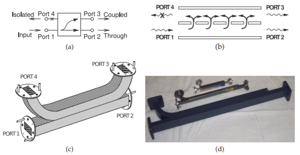
Figure \(\PageIndex{14}\): Rectangular waveguide directional couplers: (a) schematic; (b) and (c) waveguide directional coupler showing coupling slots; and (d) three directional couplers with the fourth port terminated in an integral matched load. In (d), from top to bottom: \(\text{W}\)-band, \(10\text{ cm}\) long; \(\text{Ka}\)-band, \(15\text{ cm}\) long, and \(\text{X}\)-band, \(35\text{ cm}\) long.
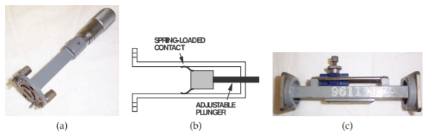
Figure \(\PageIndex{15}\): Waveguide tuners: (a) micrometer-driven variable short circuit; (b) internal details of a variable short circuit; and (c) waveguide slide tuner.