Engineering LibreTexts

1.A: Appendix- RF and Microwave Circuit Schematic Symbols

  • Page ID
    46066
  • \( \newcommand{\vecs}[1]{\overset { \scriptstyle \rightharpoonup} {\mathbf{#1}} } \) \( \newcommand{\vecd}[1]{\overset{-\!-\!\rightharpoonup}{\vphantom{a}\smash {#1}}} \)\(\newcommand{\id}{\mathrm{id}}\) \( \newcommand{\Span}{\mathrm{span}}\) \( \newcommand{\kernel}{\mathrm{null}\,}\) \( \newcommand{\range}{\mathrm{range}\,}\) \( \newcommand{\RealPart}{\mathrm{Re}}\) \( \newcommand{\ImaginaryPart}{\mathrm{Im}}\) \( \newcommand{\Argument}{\mathrm{Arg}}\) \( \newcommand{\norm}[1]{\| #1 \|}\) \( \newcommand{\inner}[2]{\langle #1, #2 \rangle}\) \( \newcommand{\Span}{\mathrm{span}}\) \(\newcommand{\id}{\mathrm{id}}\) \( \newcommand{\Span}{\mathrm{span}}\) \( \newcommand{\kernel}{\mathrm{null}\,}\) \( \newcommand{\range}{\mathrm{range}\,}\) \( \newcommand{\RealPart}{\mathrm{Re}}\) \( \newcommand{\ImaginaryPart}{\mathrm{Im}}\) \( \newcommand{\Argument}{\mathrm{Arg}}\) \( \newcommand{\norm}[1]{\| #1 \|}\) \( \newcommand{\inner}[2]{\langle #1, #2 \rangle}\) \( \newcommand{\Span}{\mathrm{span}}\)\(\newcommand{\AA}{\unicode[.8,0]{x212B}}\)

    This appendix lists the symbols commonly used with RF and microwave circuits. Symbols are from IEEE Standard 315-1975 [6]. Up until the 1970s IEEE was active in establishing standard symbols for all electrical engineering fields and in particular circuit schematic symbols to be used with microwave circuits. Since then vendors of microwave computer-aided design tools have developed their own symbols but very often a vendor tends to adopt symbols similar to those used by other vendors. However there are differences and as a result there has not been a consensus to adopt a more modern standard for microwave symbols. What is presented in this chapter follows the earlier IEEE standard where possible and for components that are not in the standard, an attempt has been made to select symbols that are in common use in technical papers.

    1.A.1 Element and Circuit Symbols

    Qualifying Property Symbol
    Adjustable clipboard_e71efe304a59c27e9dec89de5999cb87f.png
    Adjustable, continuously adjustable clipboard_e7dfb14675a50aa82e6149adb9b6becfe.png
    Adjustable, stepped clipboard_e569786b9af85de4a14e78c012d1ff5fa.png
    Linear clipboard_e3166db49fa942dbdf7d89bc683e33fed.png
    Nonlinear clipboard_e0e109a1105a55614dde26657e15b862b.png
    Positive clipboard_ec0c75774a31a9e35b74c282c2b94de3f.png
    Negative clipboard_e25b795fb0a489b257203c18eb4c01956.png

    Table \(\PageIndex{1}\): IEEE standard qualifying properties added to schematic symbols to identify a particular property.

    Component Symbol Alternate
    Analog to digital converter clipboard_e54b86683e2ea4dcee8a468b904603ca9.png
    Attenuator, fixed clipboard_eb9689f3033f0938d5d52200176161312.png
    Attenuator, balanced clipboard_e442e5f46bc45fd4649380935984a4917.png clipboard_eb497c1c06c0db53b3c22c901ff479acb.png
    Attenuator, unbalanced clipboard_ebc7917404567a8bcf2d0d03035578e9f.png clipboard_e399c000072343675b6ab45d231696b76.png
    Attenuator, variable clipboard_ed2a167be7987e0e1d56c75a44968c30d.png
    Attenuator, continuously variable clipboard_e8090792dadeb300c08e09f2ccdd52cba.png
    Attenuator, stepped clipboard_eae6842db3bf73b3e8731baf400867d2d.png
    Amplifier clipboard_ec4bbc0b6ea942b3bc15add77ec1d6a9e.png clipboard_ed5477d7bbfd84519c64ed7cd9b63de99.png
    Antenna, general clipboard_eb4d6f3157fe217bd507b737ec62a4253.png clipboard_e9e45da4e0ce0bddc672fe9868a3db560.png
    Antenna, balanced clipboard_e913350355d98dbfa9311e09aa2f3f166.png
    Antenna, dipole clipboard_e86b7bc913ac0ad88aac61ea856d0aeb4.png
    Antenna, loop clipboard_ee306204e46f35fc6d4746f7191dd496d.png clipboard_e06ab37e4519589dac863d0c5cc6e3d24.png
    Balun clipboard_e977e743f5be2646d288229482e20b54f.png
    Balun with coaxial line and dipole antenna clipboard_ec1b15902104c49c5421576ba8217e695.png
    Capacitor, general clipboard_e21da58d15bf6e369f1ef19f89e89030e.png clipboard_e4847ac48b680713b409fb1012f68d6b7.png
    Capacitor, polarized clipboard_e0e01f279b822311f4c463dcb6505ca34.png
    Capacitor, variable clipboard_e52de06689bfca64812ef486a0c4024c4.png clipboard_e242ffc6b6c4601aab0b6ace872fded02.png
    Capacitor, nonlinear clipboard_ecaf71047bc407231e48b65f347aa20c7.png
    Capacitor, shielded clipboard_e97451b5cb3a888335ca6af90549e6b87.png
    Circulator clipboard_e2eb5ddf2ec31a2e9aedfc112ea1d9c5e.png
    Coaxial cable clipboard_e9fcd7ab824d7b25d4670e758804476cd.png
    Conductive path clipboard_ea7922888c0627c9ef6d0901b38b1215c.png
    Connector, female clipboard_e5d0a8ac611dc06e9185e4fe53501d961.png
    Connector, male clipboard_ef676e6a5af5d95cce890adfb3f1c9446.png
    Contact, fixed clipboard_e3690ce811b3db85e31aea42f7629b0da.png clipboard_eaf34e146bc80d3e42889ff7f963a0f8a.png
    Contact, closed clipboard_e3f874ce433b43c084f7bd8a735a4ba5b.png
    Contact, open clipboard_eb9a789d4507f49d431f337c88116cfc4.png
    Delay clipboard_e9185d156af92ea91aa8dee25380968b8.png
    Digital-to-analog converter (DAC) clipboard_e9a8674f5139b4bb092be8a55866e1f17.png
    Element, linear (* to be replaced by designation) clipboard_ecc9fb613e22bb9e0ae0202aa901e6157.png clipboard_eb82b9aa2c9f5f20fbf149b68bb051dc7.png
    Ground, general clipboard_e93ede9203cb45d6bc0db7106c5c2fabf.png
    Ground, chassis clipboard_e13603c7093bd91385928acc6f84ae0d8.png
    Coupler clipboard_ee8e6bac29713f9cb1beef51faeeaf058.png clipboard_e68ae390513ae7ef3ca93ffa8bd034447.png
    Filter, bandpass filter (BPF) clipboard_e496964378db485e06ee1bb4afcb54ae5.png
    Filter, lowpass filter (LPF) clipboard_e275517ee619192800e71496c59e2e4a6.png
    Filter, highpass filter (HPF) clipboard_e5f9f8ad5f1e283d80914ed78d510a09c.png
    Filter, bandstop filter (BSF) clipboard_eb64d0125aaceb705965de6cc1c2b7c5d.png
    Isolator clipboard_e258f4bc04ea29972a4c6e6597403bbe3.png
    Inductor, general clipboard_ead043ca20094d7fc4d9ea328988e6b57.png clipboard_e1fbf133c2b9690a75ec3dd8f6f81f31c.png
    Inductor with magnetic core clipboard_e6ab7caedf3d7f4f5aee48bbb3ec9f83c.png
    Junction clipboard_e643752235fa46ffe97e304073f53f99b.png
    Junction of paths clipboard_e3fa13eca5535fc83b2607ec584d9590a.png
    Network, linear (*to be replaced by designation) clipboard_e4b0e887052c4fa3bed089e721c4fb9d2.png
    Open clipboard_ee91377582462dbe8fd1e717418c8bdf5.png
    Phase shifter clipboard_e83b0d3defc6760ea234f0ba0bb9d76ec.png clipboard_e2f81c67eb096227058ac54ea382fe07d.png
    Piezoelectric resonator clipboard_eb82d56cbf7d42b8904c251d90de38bcb.png
    Port clipboard_e28d4f62b05b115ea4bd82b609d1e0398.png
    Power divider clipboard_e6f889823984b7aa17f6c953c749ee4d9.png
    Radio link clipboard_edb96c9ffd932891e70b33d17c1a34f54.png
    Radio link with antennas clipboard_ee293127138e182ca7334391ff272cfec.png
    Rectifier clipboard_ed3259d1a796e20a085914df9c6926ef7.png
    Resistor, general clipboard_efe8c40d12c14fffa38b3e372025860c7.png
    Resistor, variable clipboard_e936d6903df1f41f68f3c38f6ce6f55e9.png
    Resistor, nonlinear clipboard_e71f51d5b6da5c8aa7e33074d594dd560.png
    Resistor with open path clipboard_e3945aab4c8ac8f630bd61a265a357367.png
    Resistor with short clipboard_e44d2b127b8b83c712e7bb55e8b425e30.png
    Shield clipboard_e4c587fe9c11a15a955d620f060311419.png clipboard_e0942d1636104fbe6cea2a00c490b04f0.png
    Short, movable clipboard_ece0f0bca947ba778ce7c3fe1f7904b4e.png
    Source, AC clipboard_e82a41971a178d7ace3f1b1cdb6a753f7.png
    Source, DC clipboard_e1aab4a93b891e7502bba1e9f67914731.png clipboard_eb193af6af98173f82013c3ae635eeca1.png
    Switch, multiposition clipboard_ece16b07c1c063321e5587fc11bce5fd3.png
    Test, point clipboard_e860fec79b7fa4b33846e7bd47650703c.png clipboard_e2e81eaf81516b8a9e84b74ad4bec5d0c.png
    Transformer clipboard_ebb229ec8b60aae0ca399896c983c7d2d.png
    Transformer with magnetic core clipboard_e481fcc85697a87e2ad2e9ccfe5da9b96.png
    Transformer, center tapped clipboard_ece420658fb37bceed020eac934660ac7.png
    Triax clipboard_ebe1f627044846dc5b468df13cf2415af.png
    Twinax clipboard_ecd14f6fb0143add5289bd20e2bc2197c.png
    Twinax with shield showing connection clipboard_e7261b458e66471d1f2a9bf495a02ff70.png
    Twinax with shield grounded clipboard_e777107115461e4708d667b7236f8dc31.png
    Short clipboard_e3b46bdffde2dead2abb1a72d11833be4.png
    Wire clipboard_e80fbadab5f366fd8b49a5ac48249155b.png
    Wires, connected clipboard_e1b2aeb0bd4f83fb7b4e131d8cc29dc5a.png clipboard_edcad8783a61790166ed2a9233f40ab9d.png
    Wires, unconnected, crossing clipboard_e51d758a311a2065bb01c333bb8e7ae18.png

    Table \(\PageIndex{2}\): Standard schematic symbols of RF and microwave components.

    1.A.2 Sources

    Commonly used symbols for sources.

    Component Symbol
    Voltage source clipboard_ed6cb69267c62fbbd2ce935768ef33402.png
    Current source clipboard_eacfda7e15c5ef226470d9326a92b0e79.png
    AC source clipboard_ece9df1b267f9ce22bd271060e028c098.png
    Controlled voltage source clipboard_e64a7b95e7a2a7e8e49c0505dcc09a4b2.png
    Controlled current source clipboard_e9ebc3214be704d8f313d0ad7bbc64c0d.png
    Voltage noise source clipboard_e6957fd78854909e3c40d80ceec9859d5.png
    Current noise source clipboard_ee08ba8178c6c41e71656e5e4cfb3d540.png

    Table \(\PageIndex{3}\)

    1.A.3 Diodes

    IEEE standard symbols for diodes and a rectifier [6]. (\(^{1}\)In the direction of anode (A) to cathode (K). \(^{2}\)Use symbol for general diode unless it is essential to show intrinsic region.)

    Component Symbol
    Diode, general (including Schottky)\(^{1}\) clipboard_eef96dcfdf6628ea78e7453bb8faaa50f.png
    Gunn diode\(^{1}\) clipboard_ea173dd2171505e8c686bc6c4aac8f360.png
    IMPATT diode\(^{1}\) clipboard_ebc75a8e53e710130f3a0cac8ee3c37b6.png
    PIN diode\(^{1,2}\) clipboard_e9956c1fd28c8bcb8eb78f454bf86636d.png
    Light emitting diode (LED)\(^{1}\) clipboard_eb2cd7acb01e5d766b5db56a6cd7ce767.png
    Rectifier\(^{1}\) clipboard_e983d6e164c6a68d9bbe1324f1e4b4b1d.png
    Tunnel diode\(^{1}\) clipboard_e3a0d56b246263164e5c9a0e8c60f7c29.png
    Varactor diode\(^{1}\) clipboard_eff7503e90e6668a442183112890eef87.png or clipboard_e1ad1de91ebe584d8d99981b78934981b.png
    Zener diode\(^{1}\) clipboard_e5657cbb102f4f53d57345ed404a90ff5.png

    Table \(\PageIndex{4}\)

    1.A.4 Bipolar Junction Transistor

    IEEE standard schematic symbols for bipolar junction transistors (BJT and HBT) [6] and commonly used symbols in layouts [7]. The letters indicate terminals: B (base), C (collector), E (emitter).

    Transistor IEEE Symbol Commonly Used Symbol
    BJT, pnp clipboard_e64b630d8f123b517716659f560f59471.png clipboard_e004c560e25a6ee8a24be1b16dd724198.png
    BJT, npn clipboard_e90e5178d198323df1bebcbe37949a00a.png clipboard_edaacf21a6917bb0674f3b10a82d85393.png

    Table \(\PageIndex{5}\)

    1.A.5 Junction Field Effect Transistor

    Transistor IEEE Symbol Commonly Used Symbol
    FET, pJFET clipboard_e4d8a05b382266c81b901e88474d42973.png clipboard_ec72a7f483776444439658af1a3e2f63d.png
    FET, nJFET, MESFET, HEMT clipboard_e94d1c886bde0f332288eac57fabec439.png clipboard_e57b72324a678bcb0cb0c3d61657321cc.png

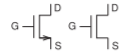
    Table \(\PageIndex{6}\): IEEE standard schematic symbols for junction field effect transistors (MESFET, HEMT, JFET) [6] and symbols more commonly used in schematics. The letters indicate terminals: G (gate), D (drain), S (source).

    1.A.6 Metal-Oxide-Semiconductor Field Effect Transistor

    Transistor IEEE Symbol Commonly used symbol (three-terminal) Commonly used symbol (four-terminal)
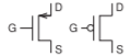
    FET, nMOS, depletion clipboard_e9cd5b258dd0fa60b13a10389b89dad0b.png clipboard_e1bc18a767ec72da1f7f49e1ac409756a.png clipboard_eb6e663f3bd37e1c43726c94c305948d9.png
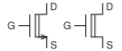
    FET, pMOS, depletion clipboard_e384b858857fb90da506e9783991e8d43.png clipboard_e9698a9d0851193c620ec9ccc1b73555a.png clipboard_e217aad8e697c97edf67f5684a4efe495.png
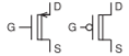
    FET, nMOS, enhancement clipboard_ec387debf81bd6f4e79205d1404fd937c.png clipboard_e6c8a8b7ef4aff3e446b52c844cf4350c.png clipboard_e42eecf48885b448fa8c507c687a30920.png
    FET, pMOS, enhancement clipboard_ef9e7a16f2a62fa5d948239ae7d56a111.png clipboard_e4ef7e39ca2d408615958717416371075.png clipboard_eb8337ecf5df08ae762a58e660d495980.png

    Table \(\PageIndex{7}\): IEEE standard schematic symbols for MOSFET transistors [6] and symbols more commonly used in schematics [7]. The MOSFET symbols are for enhancement- and depletion-mode transistors. The letters indicate terminals: G (gate), D (drain), S (source), U (bulk). Four-terminal and three-terminal common symbols are shown. The three-terminal common symbol is most often used when the bulk is connected to the most negative connection in the circuit, and the pMOSFET symbol is used when the bulk is tied to \(V_{DD}\) (the most positive connection). The bulk connection is often not shown, as it is assumed to be connected to the most negative voltage point.


    This page titled 1.A: Appendix- RF and Microwave Circuit Schematic Symbols is shared under a CC BY-NC license and was authored, remixed, and/or curated by Michael Steer.

    • Was this article helpful?