
6.11: Diode and Vacuum Sources
- Page ID
- 46135
\( \newcommand{\vecs}[1]{\overset { \scriptstyle \rightharpoonup} {\mathbf{#1}} } \)
\( \newcommand{\vecd}[1]{\overset{-\!-\!\rightharpoonup}{\vphantom{a}\smash {#1}}} \)
\( \newcommand{\dsum}{\displaystyle\sum\limits} \)
\( \newcommand{\dint}{\displaystyle\int\limits} \)
\( \newcommand{\dlim}{\displaystyle\lim\limits} \)
\( \newcommand{\id}{\mathrm{id}}\) \( \newcommand{\Span}{\mathrm{span}}\)
( \newcommand{\kernel}{\mathrm{null}\,}\) \( \newcommand{\range}{\mathrm{range}\,}\)
\( \newcommand{\RealPart}{\mathrm{Re}}\) \( \newcommand{\ImaginaryPart}{\mathrm{Im}}\)
\( \newcommand{\Argument}{\mathrm{Arg}}\) \( \newcommand{\norm}[1]{\| #1 \|}\)
\( \newcommand{\inner}[2]{\langle #1, #2 \rangle}\)
\( \newcommand{\Span}{\mathrm{span}}\)
\( \newcommand{\id}{\mathrm{id}}\)
\( \newcommand{\Span}{\mathrm{span}}\)
\( \newcommand{\kernel}{\mathrm{null}\,}\)
\( \newcommand{\range}{\mathrm{range}\,}\)
\( \newcommand{\RealPart}{\mathrm{Re}}\)
\( \newcommand{\ImaginaryPart}{\mathrm{Im}}\)
\( \newcommand{\Argument}{\mathrm{Arg}}\)
\( \newcommand{\norm}[1]{\| #1 \|}\)
\( \newcommand{\inner}[2]{\langle #1, #2 \rangle}\)
\( \newcommand{\Span}{\mathrm{span}}\) \( \newcommand{\AA}{\unicode[.8,0]{x212B}}\)
\( \newcommand{\vectorA}[1]{\vec{#1}} % arrow\)
\( \newcommand{\vectorAt}[1]{\vec{\text{#1}}} % arrow\)
\( \newcommand{\vectorB}[1]{\overset { \scriptstyle \rightharpoonup} {\mathbf{#1}} } \)
\( \newcommand{\vectorC}[1]{\textbf{#1}} \)
\( \newcommand{\vectorD}[1]{\overrightarrow{#1}} \)
\( \newcommand{\vectorDt}[1]{\overrightarrow{\text{#1}}} \)
\( \newcommand{\vectE}[1]{\overset{-\!-\!\rightharpoonup}{\vphantom{a}\smash{\mathbf {#1}}}} \)
\( \newcommand{\vecs}[1]{\overset { \scriptstyle \rightharpoonup} {\mathbf{#1}} } \)
\(\newcommand{\longvect}{\overrightarrow}\)
\( \newcommand{\vecd}[1]{\overset{-\!-\!\rightharpoonup}{\vphantom{a}\smash {#1}}} \)
\(\newcommand{\avec}{\mathbf a}\) \(\newcommand{\bvec}{\mathbf b}\) \(\newcommand{\cvec}{\mathbf c}\) \(\newcommand{\dvec}{\mathbf d}\) \(\newcommand{\dtil}{\widetilde{\mathbf d}}\) \(\newcommand{\evec}{\mathbf e}\) \(\newcommand{\fvec}{\mathbf f}\) \(\newcommand{\nvec}{\mathbf n}\) \(\newcommand{\pvec}{\mathbf p}\) \(\newcommand{\qvec}{\mathbf q}\) \(\newcommand{\svec}{\mathbf s}\) \(\newcommand{\tvec}{\mathbf t}\) \(\newcommand{\uvec}{\mathbf u}\) \(\newcommand{\vvec}{\mathbf v}\) \(\newcommand{\wvec}{\mathbf w}\) \(\newcommand{\xvec}{\mathbf x}\) \(\newcommand{\yvec}{\mathbf y}\) \(\newcommand{\zvec}{\mathbf z}\) \(\newcommand{\rvec}{\mathbf r}\) \(\newcommand{\mvec}{\mathbf m}\) \(\newcommand{\zerovec}{\mathbf 0}\) \(\newcommand{\onevec}{\mathbf 1}\) \(\newcommand{\real}{\mathbb R}\) \(\newcommand{\twovec}[2]{\left[\begin{array}{r}#1 \\ #2 \end{array}\right]}\) \(\newcommand{\ctwovec}[2]{\left[\begin{array}{c}#1 \\ #2 \end{array}\right]}\) \(\newcommand{\threevec}[3]{\left[\begin{array}{r}#1 \\ #2 \\ #3 \end{array}\right]}\) \(\newcommand{\cthreevec}[3]{\left[\begin{array}{c}#1 \\ #2 \\ #3 \end{array}\right]}\) \(\newcommand{\fourvec}[4]{\left[\begin{array}{r}#1 \\ #2 \\ #3 \\ #4 \end{array}\right]}\) \(\newcommand{\cfourvec}[4]{\left[\begin{array}{c}#1 \\ #2 \\ #3 \\ #4 \end{array}\right]}\) \(\newcommand{\fivevec}[5]{\left[\begin{array}{r}#1 \\ #2 \\ #3 \\ #4 \\ #5 \\ \end{array}\right]}\) \(\newcommand{\cfivevec}[5]{\left[\begin{array}{c}#1 \\ #2 \\ #3 \\ #4 \\ #5 \\ \end{array}\right]}\) \(\newcommand{\mattwo}[4]{\left[\begin{array}{rr}#1 \amp #2 \\ #3 \amp #4 \\ \end{array}\right]}\) \(\newcommand{\laspan}[1]{\text{Span}\{#1\}}\) \(\newcommand{\bcal}{\cal B}\) \(\newcommand{\ccal}{\cal C}\) \(\newcommand{\scal}{\cal S}\) \(\newcommand{\wcal}{\cal W}\) \(\newcommand{\ecal}{\cal E}\) \(\newcommand{\coords}[2]{\left\{#1\right\}_{#2}}\) \(\newcommand{\gray}[1]{\color{gray}{#1}}\) \(\newcommand{\lgray}[1]{\color{lightgray}{#1}}\) \(\newcommand{\rank}{\operatorname{rank}}\) \(\newcommand{\row}{\text{Row}}\) \(\newcommand{\col}{\text{Col}}\) \(\renewcommand{\row}{\text{Row}}\) \(\newcommand{\nul}{\text{Nul}}\) \(\newcommand{\var}{\text{Var}}\) \(\newcommand{\corr}{\text{corr}}\) \(\newcommand{\len}[1]{\left|#1\right|}\) \(\newcommand{\bbar}{\overline{\bvec}}\) \(\newcommand{\bhat}{\widehat{\bvec}}\) \(\newcommand{\bperp}{\bvec^\perp}\) \(\newcommand{\xhat}{\widehat{\xvec}}\) \(\newcommand{\vhat}{\widehat{\vvec}}\) \(\newcommand{\uhat}{\widehat{\uvec}}\) \(\newcommand{\what}{\widehat{\wvec}}\) \(\newcommand{\Sighat}{\widehat{\Sigma}}\) \(\newcommand{\lt}{<}\) \(\newcommand{\gt}{>}\) \(\newcommand{\amp}{&}\) \(\definecolor{fillinmathshade}{gray}{0.9}\)There are many types of sources based on special properties of diodes or of vacuum devices. This section describes some of these sources. While sources based on transistor circuits are preferred for integration and manufacturability, diode and vacuum sources are in widespread use because of either the high power that can be efficiently generated or because they operate at high frequencies beyond the reach of transistor circuits.
Two-Terminal Semiconductor Sources
Two-terminal semiconductor sources are based on exploiting the negative resistance presented at the terminals of several types of devices [37, 38, 39, 40]. They either exploit a dynamic negative resistance created in a high field region of a semiconductor due to a charge imbalance, or they exploit the finite time for carriers to cross a semiconductor region and thus produce an RF current that is out of phase with the applied voltage, thus presenting a negative RF resistance. Three representative devices are the tunnel diode, the IMPATT diode, and the Gunn diode.
Tunnel Diode
A tunnel diode is a \(\text{pn}\) junction diode in which the conduction band states on the n side are filled with electrons and these line up with empty valance band states (i.e. holes) on the \(\text{p}\) side [37, 38, 39, 40, 41, 42, 43, 44, 45, 46]. This results in a very narrow \(\text{pn}\) junction barrier. For negative voltages and small and large applied voltages the diode acts as a conventional pn junction diode with an exponential current-voltage characteristic. However, as the applied voltages increase above zero, the conduction and valance bands become more misaligned and the voltage eventually drops before increasing again. This effect is due to quantum mechanical tunnelling. This is seen in the current-voltage characteristic of the tunnel diode shown in Figure \(\PageIndex{1}\)(a), where the drop in current creates a negative dynamic resistance. Embedded in an appropriate circuit, even as simple as a parallel RLC circuit, the tunnel diode is the active element of an RF oscillator. Usually a Gunn diode has a very high dopant concentration so that the reverse breakdown voltage is very low.
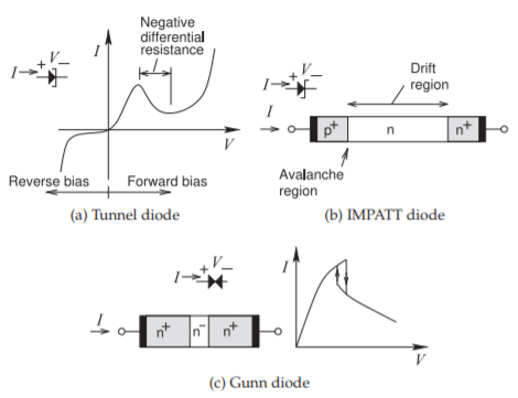
Figure \(\PageIndex{1}\): Two terminal semiconductor sources.
IMPATT Diode
An IMPATT diode (IMPact ionization Avalanche Transit-Time) produces high power and throughout the history of its use it has produced the highest power levels at the highest frequency, up to \(1000\text{ GHz}\), of any semiconductor device [37, 38, 39, 40, 47, 48, 49, 50, 51].
The IMPATT diode is the most important of the transit time semiconductor diodes, see Figure \(\PageIndex{1}\)(b). In transit time devices the generation of charge carriers is concentrated in one narrow region of the diode. In an IMPATT diode, a high field at the boundary between a highly doped n region, the \(\text{n}^{+}\) region, and a lightly doped n region leads to avalanche multiplication producing holes and electrons. The holes are quickly collected by an adjacent metal contact and the electrons transit through a drift region with usually intrinsic doping and a constant field. If the drifting electrons are sufficiently delayed, then the RF current through the device will be out of phase with the applied RF voltage (superimposed on a biasing DC voltage) and a negative RF resistance is presented at the device terminals. The roles of the holes and electrons can also be exchanged. Thus the IMPATT diode can be used as the active component of an oscillator [52]. They can be used in an amplifier as a reflection device having a reflection coefficient greater than one [53]. However, the oscillating signal produced has high noise due to the underlying avalanche process.
Other effects can produce charges that eventually drift and produce a negative RF resistance. An example is a TUNNETT diode that injects charges through tunneling [54, 55]. Another device is the TRAPATT diode (trapped plasma avalanche transit time diode), a pn junction diode, where the carrier injection results from a trapped space-charge plasma formed within the junction region [42, 56].
Gunn Diode
A Gunn diode is also called a transferred electron device or a Gunn effect device. While strictly not a diode as there is not a junction, the name Gunn diode has become common usage because there are two electrodes. The structure and current-voltage characteristic of a Gunn diode are shown in Figure \(\PageIndex{1}\)(c) [37, 38, 39, 40, 57, 58, 59, 60, 61]. The device has three \(\text{n}\)-type regions: two heavily doped \(\text{n}^{+}\) regions at each contact, separated by a lightly doped \(\text{n}^{−}\) region. When a voltage is applied to the device, most of the voltage is across the \(\text{n}^{−}\) region and the device acts like a resistor with the current through the Gunn diode proportional to the voltage across it. At higher voltages the conductivity of the \(\text{n}^{−}\) region drops and the current drops, so that there is a region of negative dynamic resistance.
Vacuum Devices
Some microwave systems use vacuum tubes to obtain high RF powers; the most common vacuum tube devices are reviewed here.
Magnetron
The magnetron is the original device used for generating microwave power and was invented during World War II for use in radar equipment. It is most commonly used in microwave ovens, where it is the most efficient means of producing microwave power at \(2.4\text{ GHz}\). It is used in military systems today to produce megawatts of pulsed RF power and is used to generate substantial power up to a few terahertz [62, 63, 64, 65]. In a magnetron a circular chamber, containing the cathode, is surrounded by and connected to a number of resonant cavities. The walls of the chamber are the anode. The cavity dimensions determine the frequency of the output signal. A strong constant magnetic field in the chamber causes electrons that want to flow from the cathode to the anode to rotate. As the electrons pass the entrance of the circular cavities, the electrons interact with the EM field in the cavity, enhancing the field at a characteristic frequency, which is the frequency of oscillation of the magnetron.
Klystron
The klystron is a long, narrow vacuum tube with an electron gun (the cathode) at one end and an anode at the other [66, 67, 68, 69]. In between is a series of doughnut-shaped resonant cavities aligned so that the electron beam from the cathode passes through the hole. As the beam passes the cavities, small changes in the electron beam affect the EM field in the cavities. The EM fields in the cavities begin to oscillate, which in turn affect the passing electron beam. A feedback effect results, and when the last and first resonant cavities are connected, a large oscillating microwave signal is produced.
Traveling Wave Tube and Backward Wave Oscillator
A traveling wave tube (TWT) is a long vacuum tube with an electron gun (the cathode) at one end and a collector (the anode) at the other. The electron beam produced by the gun travels down the center of a long wire helix [70, 71, 72, 73, 74, 75]. An excitation coupling probe, an antenna, placed near the cathode introduces a microwave signal. This modulates the electron beam, which in turn induces an RF current in the helix. The helix is designed so that the EM signal supported by the helix travels at the same speed as the electron beam so that the electron beam and EM signal guided by the helix continuously interact. Thus the RF current in the helix as well as the RF field grow in strength along the tube. An output probe at the anode end of the tube couples to the RF field and delivers an amplified version of the input RF signal. As an amplifier the TWT is called a traveling wave tube amplifier (TWTA).
In the TWT the helix slows the RF signal down to match the speed of the electrons and so the helix is called a slow-wave structure. Another tube device that uses a slow-wave structure is the backward wave oscillator (BWO). However, in the BWO the beam is directed against the traveling wave supported by the helix.