
3.5: Case Study- Wideband Amplifier Design
- Page ID
- 46039
In this section an \(X\)-band wideband low-noise amplifier is designed.\(^{1}\) The topology of the amplifier is shown in Figure \(\PageIndex{1}\), and this is the same topology used in narrowband amplifier design. The design specification is for a maximum noise figure (NF) of \(1\text{ dB}\) and a gain of \(14 ± 1\text{ dB}\) from \(8\text{ GHz}\) to \(12\text{ GHz}\).
3.5.1 Transistor Properties
The transistor chosen is the packaged NEC NE32400A transistor and its parameters are given in Table \(\PageIndex{1}\) in what is called the Touchstone\(^{\circledR}\) format used by microwave simulators. The file begins with a number of comment lines (identified by ‘!’) followed by the option line:
# <frequency unit> <parameter> <format> R <n>
where the <frequency unit> is \(\text{GHz}\), <parameter> specifies the kind of network parameter data, and here \(S\) is scattering parameters. The <format>, MA, indicates that the data is in magnitude-angle(degrees) format, and the <n> term is \(50\), indicating that the \(S\) parameters are normalized to \(50\:\Omega\). The line of data is ordered as \(f,\: |S_{11}|,\: \angle S_{11},\) \(|S_{21}|,\: \angle S_{21}\), \(|S_{12}|,\: \angle S_{12}\), \(|S_{22}|\), and \(\angle S_{22}\). The second set of data contains the noise parameters and there are five entries for each frequency arranged as frequency (using the previously specified units), the minimum noise figure \(\text{NF}_{\text{min}}\) (in \(\text{dB}\)), then \(|\Gamma_{\text{opt}}|\), \(\angle\Gamma_{\text{opt}}\), and \(r_{n}/50\). These are the noise parameters used with two-port amplifiers as described in Section 4.3.6 of [6] with \(\text{NF}_{\text{min}} = 10 \log(F_{\text{min}})\) and \(\Gamma_{\text{opt}}\) being the reflection coefficient of \(\Gamma_{\text{opt}}\) referenced to \(Y_{0}\) (\(= 0.02\text{ S}\) here).
The \(S\) parameters of the transistor are plotted in Figure \(\PageIndex{2}\). \(S_{11},\: S_{12},\) and \(S_{22}\) are plotted on a Smith chart in Figure \(\PageIndex{2}\)(a). However, \(S_{21}\) is greater than one and so this is plotted on a polar plot in Figure \(\PageIndex{2}\)(b). All of the \(S\) parameters vary significantly with frequency. In Figure \(\PageIndex{2}\)(a) the locus of \(S_{11}\) from \(8\text{ GHz}\) to \(12\text{ GHz}\) is highlighted and the segment is labeled \(\mathsf{A}\). Ideal matching would require that the reflection coefficient, \(\Gamma_{S}\), looking into the lossless input matching network from the transistor be the complex conjugate of \(S_{11}\) (if Port 2 of the transistor is terminated in \(50\:\Omega\)).
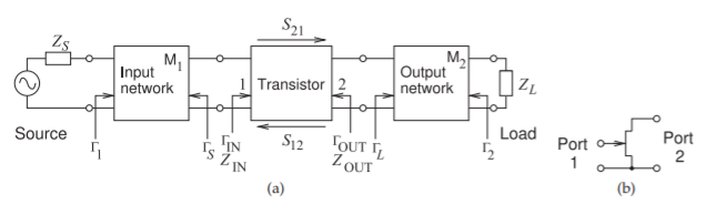
Figure \(\PageIndex{1}\): Wideband amplifier: (a) topology; and (b) port definition for transistor parameters.
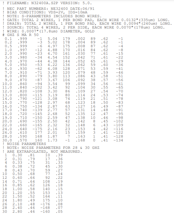
Table \(\PageIndex{1}\): \(S\) parameter data file for a packaged NE32400A HJFET (heterojunction FET) transistor. # GHZ S MA R 50 indicates frequency in \(\text{GHz}\), \(S\) parameters in magnitude-angle(degrees) format, and reference to \(50\:\Omega\). The \(S\) parameter data are \(f(\text{GHz})\), magnitude and angle of \(S_{11},\: |S_{21}|,\: S_{12},\: |S_{22}|\). Noise data are \(f(\text{GHz})\), \(\text{NF}_{\text{min}}\) \((\text{dB})\), \(|\Gamma_{\text{opt}}|\), \(\text{ang}(\Gamma_{\text{opt}})\) (in degrees), and \(r_{n}/50\).
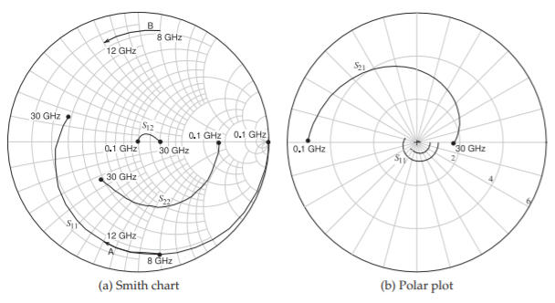
Figure \(\PageIndex{2}\): \(S\) parameters of the N32400A transistor. \(|S_{21}|\) exceeds unity and is shown on a polar plot in (b) where \(2,\: 4,\) and \(6\) indicate the magnitudes (radii) of constant \(|\Gamma |\) circles.
Thus the locus of the optimum \(\Gamma_{S}\) is shown as segment \(\mathsf{B}\) in Figure \(\PageIndex{2}\)(a). Note that \(\Gamma_{S}\) rotates in the counterclockwise direction with increasing frequency. However, the input reflection coefficient of a simple matching network would rotate in the clockwise direction. Thus a reasonable match will only be achieved over a very narrow bandwidth. The output matching network situation is similar. The ideal matching network must have an input reflection coefficient that is counter to that of a simple network. So this illustrates the big difference between wideband and narrowband amplifier design. The matching networks must be designed to present the required complex conjugate impedance over a broad range of frequencies.
Another design task is simultaneously minimizing noise. The noise data of the transistor is plotted in Figure \(\PageIndex{3}\). Figure \(\PageIndex{3}\)(a) plots the value of \(\Gamma_{S}\) \((= \Gamma_{\text{opt}})\) required to achieve the minimum noise figure. The points are just \(\Gamma_{\text{opt}}\) at different frequencies. These points do not coincide with the \(\Gamma_{S}\) for optimum matching as shown in Figure \(\PageIndex{2}\)(a). So a compromise is needed. This compromise step is guided by the noise figure circles. Figure \(\PageIndex{2}\)(b) plots the noise figure circles when the noise figure is \(0.25\text{ dB}\) higher than \(\text{NF}_{\text{min}}\). For example, at one frequency, if \(\Gamma_{S}\) is on the circle for that frequency, the noise figure will be \(0.25\text{ dB}\) higher than \(\text{NF}_{\text{min}}\). If \(\Gamma_{S}\) is inside the circle the noise figure will be less than \(0.25\text{ dB}\) above \(\text{NF}_{\text{min}}\).
A more complete set of noise figure circles at \(10\text{ GHz}\), the middle of the amplifier band, is shown in Figure \(\PageIndex{4}\). \(\text{NF}_{\text{min}}\) is \(0.50\text{ dB}\) and the noise figure circles are in \(0.1\text{ dB}\) steps.
Another consideration affecting the choice of matching networks is the stability of the amplifier. The input and output stability circles for the transistor are shown in Figure \(\PageIndex{5}\) starting at \(2\text{ GHz}\) and up to \(30\text{ GHz}\). For the transistor to be unconditionally stable, \(\Gamma_{S}\), must lie in the unconditionally stable region of the Smith chart. The stable regions are shown in Figure
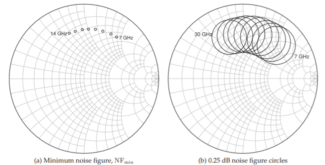
Figure \(\PageIndex{3}\): Noise characteristic from \(7\) to \(14\text{ GHz}\) in \(1\text{ GHz}\) steps plot on the input (\(\Gamma_{S}\)) plane. \(\text{NF}_{\text{min}} = 0.38\text{ dB}\), \(0.41\text{ dB}\), \(0.43\text{ dB}\), \(0.47\text{ dB}\), \(0.50\text{ dB}\), \(0.55\text{ dB}\), \(0.60\text{ dB}\), \(0.66\text{ dB}\), and \(0.71\text{ dB}\) from \(7\) to \(14\text{ GHz}\) in \(1\text{ GHz}\) steps. The noise figure on each circle is \(\text{NF}_{\text{min}} + 0.25\text{ dB}\).
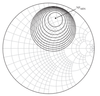
Figure \(\PageIndex{4}\): Noise figure circles at \(10\text{ GHz}\) where \(\text{NF}_{\text{min}} = 0.50\text{ dB}\). Circles have \(0.1\text{ dB}\) steps so that the inner-most circle indicates the values of \(\Gamma_{S}\) that achieve \(\text{NF} = 0.6\text{ dB}\).
\(\PageIndex{5}\)(a) at all frequencies. Similarly, \(\Gamma_{L}\) must lie in the stable region of the Smith chart in Figure \(\PageIndex{5}\)(b) at all frequencies. The final consideration is the maximum available gain, \(G_{\text{MAX}}\). The \(G_{\text{MAX}}\) circles are shown in Figure \(\PageIndex{6}\). At \(8\text{ GHz }G_{\text{MAX}} = 16.6\text{ dB}\) and it reduces to \(14.8\text{ dB}\) at \(12\text{ GHz}\). This further complicates design as the gain of the final amplifier should be flat across the band and not monotonically decreasing.
So the complete design problem is to determine the matching network topology and then develop the input and output matching networks that meet all of the constraints implied by the stability circles, the noise figure
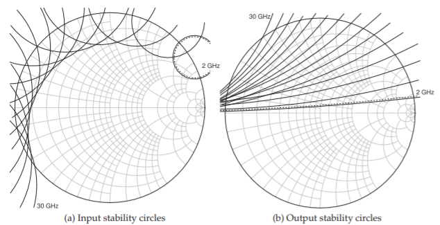
Figure \(\PageIndex{5}\): Stability circles in \(2\text{ GHz}\) steps starting at \(2\text{ GHz}\) and continuing up to \(30\text{ GHz}\). The potentially unstable region is indicated by the dashed line on the \(2\text{ GHz}\) circle.
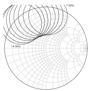
Figure \(\PageIndex{6}\): Maximum available gain, \(G_{\text{MAX}}\), circles. \(G_{\text{MAX}} = 17.0\text{ dB}\), \(16.5\text{ dB}\), \(16.0\text{ dB}\), \(15.5\text{ dB}\), \(15.2\text{ dB}\), \(14.8\text{ dB}\), \(14.5\text{ dB}\), \(14.1\text{ dB}\) at \(7\) to \(14\text{ GHz}\) in \(1\text{ GHz}\) steps.
circles, and the \(G_{\text{MAX}}\) circles.
3.5.2 Negative Image Design
A successful strategy for wideband design is the negative image amplifier design technique. The development begins by considering the fundamental input and output impedances of the transistor. The input of a transistor can be approximated as a resistance in series with a capacitance. The output of the transistor appears as a capacitance in parallel with a resistance. So a simple matching strategy is to consider an input matching network that presents a negative series capacitance (the image) to the
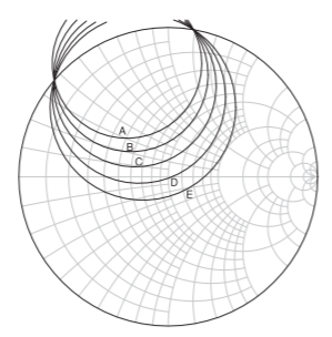
Figure \(\PageIndex{7}\): Maximum available gain, \(G_{\text{MAX}}\), circles at \(10\text{ GHz}\) in \(1\text{ dB}\) steps. The central circle has \(G_{\text{MAX}} =15.5\text{ dB}\).
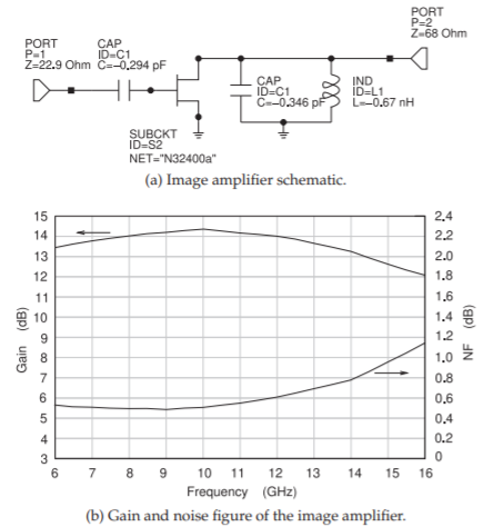
Figure \(\PageIndex{8}\): Amplifier using negative image model.
input of the transistor and a negative shunt capacitance to the output of the transistor. Such an amplifier is shown in Figure \(\PageIndex{8}\)(a). The output matching network also includes a negative shunt inductance that cancels the bondwire inductance of the packaged transistor. The input and output port impedances were adjusted to achieve the required gain. The values of the input and output port impedances as well as of the three reactive elements can be optimized or adjusted using the manual tuning feature in most microwave simulators. Tuning is a useful feature that provides considerable
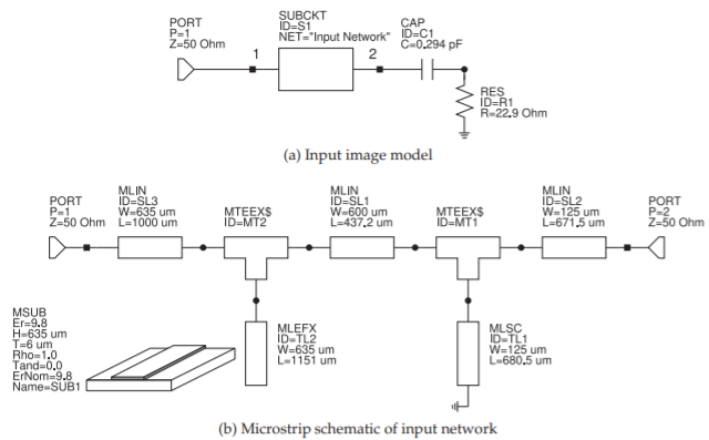
Figure \(\PageIndex{9}\): Microstrip realization of the input matching network using a microstrip substrate, \(\mathsf{MSUB}\). The layout begins with a port element \(\mathsf{PORT\: 1\: (P=1)}\) with a reference impedance of \(50\:\Omega\). The \(\mathsf{MLIN}\) element is a microstrip line with width \(\mathsf{W}\) and length \(\mathsf{L}\); the \(\mathsf{MTEEX$}\) element models a microstrip tee and supports the shunt connection of the \(\mathsf{MLEFX}\) element, which is an open-circuited microstrip line with end effects modeled; another line and tee connects a shorted stub, the \(\mathsf{MLSC}\) element; then another line; and finally a second \(\mathsf{PORT}\) element.
insight. The trade-offs are not always easy to make without using the image amplifier technique.
The noise and gain of the image amplifier of Figure \(\PageIndex{8}\)(a) are shown in Figure \(\PageIndex{8}\)(b). While the gain and noise figure do not meet the specification (\(13\text{ dB}\) gain and \(\text{NF }< 1\text{ dB}\)), they are very close and it can be expected that optimization will achieve the required design.
At this stage the topologies of the input and output matching networks need to be selected since negative inductances and capacitors are not available. There are several ways this can be done. One way is to develop transfer function descriptions of the impedances of the input (and output) network seen from the transistor. The impedance functions can then be synthesized and developed as if they were filters. This can be a long process, but sometimes it is the only way to meet demanding specifications. Very often the topology can be adopted from an earlier design or from a design reported in a publication. The topology chosen here for the input network is shown in Figure \(\PageIndex{9}\)(b). (The theory behind this topology is described in Section 7.7 of [6].) The parameters of the input matching network are optimized using the input image model shown in Figure \(\PageIndex{9}\)(a). However, the sign of the negative capacitance in the input circuit of Figure \(\PageIndex{8}\)(a) is changed. The series connection of the \(0.294\text{ pF}\) capacitor in series with
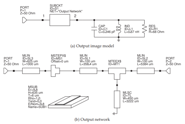
Figure \(\PageIndex{10}\): Realization of the output network.
the \(22.9\:\Omega\) resistor approximates the input impedance of the (terminated) transistor. More specifically, it is the impedance that will result in the gain and noise profile in Figure \(\PageIndex{8}\)(b). The goal in realizing the input matching network is to minimize the input reflection coefficient (normalized to \(50\:\Omega\)) at the input port. A similar approach is used in developing the output matching network, shown in Figure \(\PageIndex{10}\). Following optimization, the input reflection coefficients at Port \(1\) of the matching networks terminated in the image networks are shown in Figure \(\PageIndex{11}\).
3.5.3 Final Design
The input and output matching networks are connected to the transistor as shown in Figure \(\PageIndex{12}\) and then the complete amplifier is optimized. The parameters of the optimized input and output matching networks using the complete transistor model are given in Figures \(\PageIndex{9}\)(b) and \(\PageIndex{10}\)(b), and the complete layout is shown in Figure \(\PageIndex{13}\). The gain and noise performance of the completed design is given in Figure 3.6.1. This wideband amplifier topology achieves a bandwidth up to one-half octave (e.g. \(8–12\text{ GHz}\)).
In some cases, although not required here, it is necessary to introduce feedback from the output to the input of the transistor. This is often a simple circuit such as a cascade of a capacitor, an inductor, and a transmission line. The feedback network provides frequency-dependent feedback that flattens the gain response. A resistor can be also included in the feedback network to manage stability.
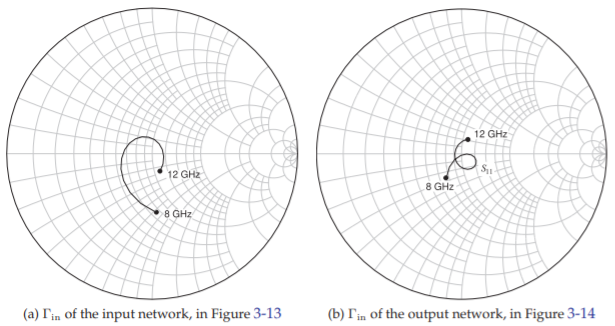
Figure \(\PageIndex{11}\): Reflection coefficient looking into Port 1 of the input and output matching networks terminated in the corrected image network.
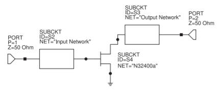
Figure \(\PageIndex{12}\): Final amplifier.
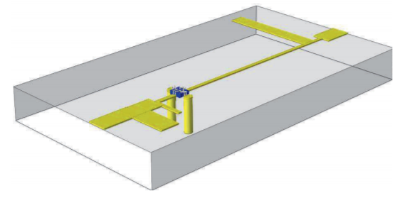
Figure \(\PageIndex{13}\): Final layout of the \(X\)-band LNA. The input is on the left and the output on the right.
Footnotes
[1]  Design Environment Project File: X Band LNA.emp