
5.9: Case Study- Oscillator Phase Noise Analysis
- Page ID
- 46102
In this section the oscillator shown in Figure 5.8.3 is modeled and simulated in the time-domain [25, 26, 36]. The circuit includes three nonlinear devices, two identical BJTs and one varactor, which must be modeled. The process of developing a device model involves fitting the coefficients of a physically based model to measured characteristics. The development of models of the noise sources also requires fitting some noise parameters to measurements.
Device Modeling
The physical model used with each of the BJTs is shown in Figure \(\PageIndex{1}\) along with thermal, shot, and flicker noise sources. The Gummel-Poon BJT model was used with parameters provided by the manufacturer. The thermal noise sources, \(i_{t,rb}\), \(i_{t,rc}\), and \(i_{t,re}\), are associated with the parasitic resistors at the collector, base, and emitter, respectively. The thermal noise current source models are
\[\label{eq:1}i_{t,rc}=\sqrt{\frac{2kT}{R_{c}}}\xi_{c},\quad i_{t,rb}=\sqrt{\frac{2kT}{R_{bb}}}\xi_{b}\quad\text{and}\quad i_{t,re}=\sqrt{\frac{2kT}{R_{e}}}\xi_{e} \]
where \(\xi_{c},\:\xi_{b},\) and \(\xi_{e}\) are sequences of white noise generated by the logistic map of Equation (5.8.12) with \(\lambda = 4\). The \(\xi_{c}\)s have values between \(0\) and \(1\). In this case the model is based on physical mechanisms and fitting of the noise model to measurements is not required.
Based on the development in [55] and [56], when the transistor is in the forward active region, minority carriers diffuse and drift across the base into the base-collector region. Since there is an electric field, the charges undergo acceleration when they enter the collector-base depletion region and are swept to the collector. This is a random process and is the source of shot noise in the collector. Recombination effects in the base-emitter region and carrier injection from the base into the emitter are also random processes contributing to shot noise in the base and emitter, respectively. Thus there are three shot noise current sources, \(i_{s,ce}\), \(i_{s,be}\), and \(i_{s,bc}\), which are proportional to the instantaneous collector-emitter, base-emitter, and base-collector currents, respectively. They are modeled as follows:
\[\label{eq:2}i_{s,ce}=\sqrt{e|i_{ce}|}\xi_{ce},\quad i_{s,be}=\sqrt{e|i_{be}|}\xi_{be},\quad\text{and}\quad i_{s,bc}=\sqrt{e|i_{bc}|}\xi_{bc} \]
where \(\xi_{ce},\:\xi_{be}\), and \(\xi_{bc}\) are white noise sequences between \(0\) and \(1\) and generated by the logistics map with \(\lambda = 4\), and \(e\) is the elementary charge.
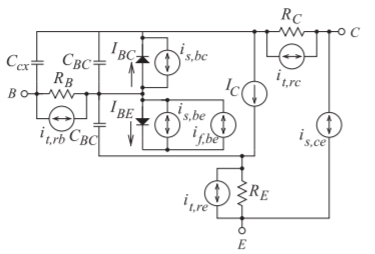
Figure \(\PageIndex{1}\): The Gummel-Poon BJT model, along with noise sources.
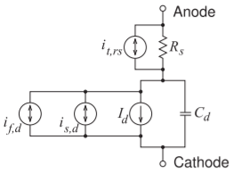
Figure \(\PageIndex{2}\): The p-n junction diode model with noise source.
Although there is more than one known source of flicker noise in a BJT [57], it has been shown that the dominant source of flicker noise can be modeled as a single noise current between the base and emitter terminals. It is a function of the instantaneous base-emitter recombination current [58] and so the flicker noise source is
\[\label{eq:3}i_{f,be}=k_{f}\sqrt{|i_{be}|^{\alpha}}\xi_{f} \]
Here \(\xi_{f}\) is between \(0\) and \(1\) and is a sequence generated by the logarithmic map in Equation (5.8.15) and \(\alpha\) controls the dependence of the flicker noise component on the non-ideal base current; here \(\alpha\) is set to \(2\). The logarithmic map sequence, \(\xi_{f}\), is parameterized by \(\beta\), which was fit to noise measurements yielding \(\beta = 0.000005\). The other parameter, \(k_{f}\), sets the amplitude of the flicker noise and fitting to noise data yielded \(k_{f} = 0.001\). The same flicker noise parameters were used with both BJTs. All of the noise sources were uncorrelated and this was achieved by randomly choosing initial seeds of each sequence, the \(\xi\)s.
The diode model is shown in Figure \(\PageIndex{2}\). The noisy model of the diode includes a thermal current source for the parasitic resistance, a shot noise current source, and a flicker noise current source that is dependent on the current flowing through the diode [56]. The diode’s thermal, shot, and flicker noise current sources are
\[\label{eq:4}i_{t,rs}=\sqrt{\frac{2kT}{R}}\xi_{t},\quad i_{s,d}=\sqrt{ei_{d}}\xi_{s},\quad\text{and}\quad i_{f,d}=k_{fd}\sqrt{i_{d}^{\alpha}}\xi_{f} \]
respectively. Here the parameter \(k_{fd}\) is the scaling coefficient for the diode flicker noise and \(\alpha\) controls the dependence of the flicker noise component on the current in the diode. As with the BJT, \(\alpha = 2\) in the simulations reported here. The parameter \(\beta\) controls the slope of the autocorrelation characteristic. As before, the random variables \(\xi_{t}\) and \(\xi_{s}\), describing the thermal and shot noise processes, were generated using the logistic map, and \(\xi_{f}\), describing the flicker noise process, was generated using the logarithmic map. The amplitude of the flicker noise source was fit to measurements and the same \(\beta = 0.00005\) parameter was used as was determined for the BJT model.
The noise model of the oscillator is completed by modeling the thermal noise current of each resistor as in Equation \(\eqref{eq:1}\).
Oscillator Simulation
The VCO circuit of Figure 5.8.3 was simulated in the time domain using the transient simulator described in [25] and [26]. In the circuit model there are a total of three flicker noise parameters fit to measurements, \(k_{f}\) for the BJTs, \(k_{fd}\)
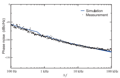
Figure \(\PageIndex{3}\): Phase noise comparison between data and experiment with bias voltage at \(0\text{ V}\).
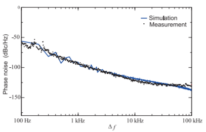
Figure \(\PageIndex{4}\): Phase noise comparison between data and experiment with bias voltage at \(6\text{ V}\).
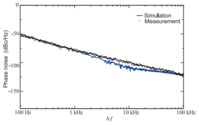
Figure \(\PageIndex{5}\): Phase noise comparison between data and experiment with bias voltage at \(12\text{ V}\).
for the diode, and the same value of \(\beta\) was used for the BJTs and the diode. Thus there are three noise parameters to be set in the VCO circuit. These were unchanged in simulations of the VCO with different varactor bias voltages. These are the only noise parameters that are not fixed by the device currents and parasitic resistance values. The phase noise output following simulation was Fourier analyzed yielding the phase noise results shown in Figures \(\PageIndex{3}\) to \(\PageIndex{5}\). These measured results were also presented in Figures 5.8.4 and 5.8.5, where the phase noise slopes were identified as \(f^{0},\: f^{−1},\) \(f^{−2}\), and \(f^{−3}\). So the simulated phase noise results in Figures \(\PageIndex{3}\) to \(\PageIndex{5}\) correctly calculate the various phase noise slopes and crossover frequencies for diverse varactor tuning conditions.