
5.12: Exercises
- Page ID
- 46081
\( \newcommand{\vecs}[1]{\overset { \scriptstyle \rightharpoonup} {\mathbf{#1}} } \) \( \newcommand{\vecd}[1]{\overset{-\!-\!\rightharpoonup}{\vphantom{a}\smash {#1}}} \)\(\newcommand{\id}{\mathrm{id}}\) \( \newcommand{\Span}{\mathrm{span}}\) \( \newcommand{\kernel}{\mathrm{null}\,}\) \( \newcommand{\range}{\mathrm{range}\,}\) \( \newcommand{\RealPart}{\mathrm{Re}}\) \( \newcommand{\ImaginaryPart}{\mathrm{Im}}\) \( \newcommand{\Argument}{\mathrm{Arg}}\) \( \newcommand{\norm}[1]{\| #1 \|}\) \( \newcommand{\inner}[2]{\langle #1, #2 \rangle}\) \( \newcommand{\Span}{\mathrm{span}}\) \(\newcommand{\id}{\mathrm{id}}\) \( \newcommand{\Span}{\mathrm{span}}\) \( \newcommand{\kernel}{\mathrm{null}\,}\) \( \newcommand{\range}{\mathrm{range}\,}\) \( \newcommand{\RealPart}{\mathrm{Re}}\) \( \newcommand{\ImaginaryPart}{\mathrm{Im}}\) \( \newcommand{\Argument}{\mathrm{Arg}}\) \( \newcommand{\norm}[1]{\| #1 \|}\) \( \newcommand{\inner}[2]{\langle #1, #2 \rangle}\) \( \newcommand{\Span}{\mathrm{span}}\)\(\newcommand{\AA}{\unicode[.8,0]{x212B}}\)
- Draw the schematic of an op-amp-based Hartley oscillator circuit.
- Consider the circuit below. This is the equivalent circuit of an active device with a negative conductance \(= 1/R_{D}\) connected to a tank circuit comprising capacitor \(C_{T}\) and inductor \(L_{T}\), and then a load \(R_{L}\). The oscillation amplitude will adjust so that \(R_{D} = R_{L}\).
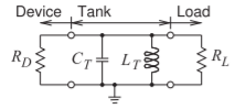
Figure \(\PageIndex{1}\)
- Write down a formula for the oscillation frequency \(f_{0}\).
- What is \(f_{0}\) if \(C_{T} = 1\text{ pF}\) and \(L_{T} = 1\text{ nH}\)?
- The circuit below is the equivalent circuit of a reflection oscillator with a negative conductance \(= 1/R_{D}\) connected to a tank circuit \(C_{T} = 0.1\text{ pF}\) and \(L_{T} = 0.5\text{ nH}\). What is the oscillation frequency assuming that there is sufficient negative conductance for oscillation to occur?
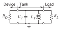
Figure \(\PageIndex{2}\)
- The circuit below is the equivalent circuit of a reflection oscillator with a negative conductance \(= 1/R_{D}\) connected to a tank circuit with a capacitance \(C_{T} = 1\text{ pF}\) and inductance \(L_{T} = 1\text{ nH}\). The load consists of a capacitor \(C_{L}\) in parallel with a resistor \(R_{L}\). The oscillation amplitude will adjust so that \(R_{D} = R_{L}\).
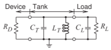
Figure \(\PageIndex{3}\)
- Write down a symbolic formula for the oscillation frequency \(f_{0}\).
- What is \(f_{0}\) if \(C_{L} = 0.2\text{ pF}\) and \(R_{L} = 50\:\Omega\)?
- The circuit below is the equivalent circuit of a reflection oscillator with a negative conductance \(= 1/R_{D}\) connected to a tank circuit \(C_{T} = 0.1\text{ pF}\) and \(L_{T} = 0.5\text{ nH}\). The capacitance of the load is \(C_{L} = 0.05\text{ pF}\) and the load resistance is \(50\:\Omega\). What is the oscillation frequency assuming that there is sufficient negative conductance for oscillation to occur?
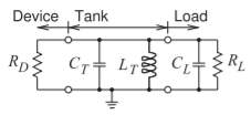
Figure \(\PageIndex{4}\)
- The circuit below is the equivalent circuit of a reflection oscillator with a negative conductance \(= 1/R_{D}\) connected to a tank circuit with a capacitance \(C_{T} = 1\text{ pF}\) and inductance \(L_{T} = 1\text{ nH}\). The load consists of a capacitor \(C_{L} = 0.2\text{ pF}\) in parallel with a resistor \(R_{L} = 50\:\Omega\). Between the tank circuit is a \(3\text{ dB}\) \(50\:\Omega\) attenuator (i.e., the system is designed for system impedance of \(50\:\Omega\)). The oscillation amplitude will adjust so that \(R_{D} = R_{L}\).
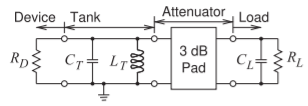
Figure \(\PageIndex{5}\)
- Ignore the load capacitor \(C_{L}\), what is the frequency of oscillation, \(f_{0}\), of the oscillator?
- From now on consider the load capacitance. What is the oscillation frequency without the attenuator?
- At the frequency calculated in (a), what is the admittance looking into the attenuator from the tank circuit with the load comprising \(C_{L}\) and \(R_{L}\)? [Hint use the resistive PI network equivalent of the attenuator.]
- What is the equivalent shunt resistor and capacitor circuit looking into the attenuator from the oscillator? This is the effective load seen by the active device and tank circuit.
- What is the oscillation frequency with the attenuator and the RC load?
- Using your results above, discuss the effect of the attenuator on reducing the sensitivity of oscillation on the loading conditions.
- The circuit below is the equivalent circuit of a reflection oscillator with a negative conductance \(= 1/R_{D}\) connected to a tank circuit with a capacitance \(C_{T} = 1\text{ pF}\) and inductance \(L_{T} = 1\text{ nH}\). The load consists of a capacitor \(C_{L} = 0.2\text{ pF}\) in parallel with a resistor \(R_{L} = 50\:\Omega\). Between the tank circuit is a \(3\text{ dB }50\:\Omega\) attenuator (ti.e., the system is designed for system impedance of \(50\:\Omega\)) and a bandpass filter with an insertion loss at the oscillation frequency of \(2\text{ dB}\). The oscillation amplitude will adjust so that \(R_{D} = R_{L}\).
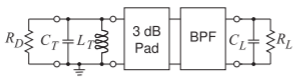
Figure \(\PageIndex{6}\)
- Ignore the load capacitor \(C_{L}\), what is the frequency of oscillation, \(f_{0}\), of the oscillator?
- From now on consider the load capacitance. What is the oscillation frequency without the attenuator and bandpass filter?
- At the frequency calculated in (a), what is the admittance looking into the attenuator from the tank circuit with the bandpass filter and the load comprising \(C_{L}\) and \(R_{L}\)? [Hint: Consider that the effect of the insertion loss of the filter is an attenuation. Consider using a resistive PI network equivalent of the attenuator plus bandpass filter.]
- What is the equivalent shunt resistor and capacitor circuit looking into the attenuator for the oscillator? This is the effective load seen by the active device and tank circuit.
- What is the oscillation frequency with the attenuator and the RC load?
- A reflection oscillator is shown below along with the \(\Gamma_{r}\) and \(\Gamma_{d}\) loci plotted on a Smith chart. \(\Gamma_{r}\), the reflection coefficient looking into the resonator, rotates clockwise as frequency increases. \(\Gamma_{d}\), the reflection coefficient of the active device, is amplitude dependent but is frequency independent. The arrowed \(\Gamma_{d}\) curve plots the loci of \(\Gamma_{d}\) as amplitude increases. [Hint: Consider Figure 5.5.4.]
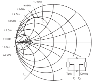
Figure \(\PageIndex{7}\)
- On the \(\Gamma_{r}\) plane show the region of the Smith Chart identifying oscillation.
- On the \(\Gamma_{d}\) plane show the region of the Smith Chart identifying oscillation.
- What is the frequency of oscillation?
- Consider an oscillator that can be modeled as shunt connections of a linear conductance, \(G_{r}\), a linear susceptance, \(B_{r}\), a nonlinear or device conductance, \(G_{d}\), and a nonlinear or device susceptance, \(B_{d}\).
- Draw the circuit.
- Using \(G_{r},\: B_{r},\: G_{d},\) and \(B_{d}\), write down the Kurokawa oscillator condition that establishes stable single frequency oscillation.
- What are common design choices \(G_{r},\: B_{r},\: G_{d},\) and \(B_{d}\) made that simplify the Kurokawa oscillator condition? Write down the resulting simplified Kurokawa oscillation condition.
- An oscillator has a linear conductance, \(G_{r}\), a linear susceptance, \(B_{r}\), a nonlinear or device conductance, \(G_{d}\), and a nonlinear or device susceptance, \(B_{d}\), all in shunt. The reflection coefficient looking into the linear network is \(\Gamma_{r}\) and the reflection coefficient looking into the device is \(\Gamma_{d}\).
- Use a Smith chart sketch to show the loci of the linear and nonlinear admittances (or equivalently their reflection coefficients \(\Gamma_{r}\) and \(\Gamma_{d}\)) for the case when loss in the linear network is low (i.e. \(G_{r}\approx 0\)). Do this when the oscillating signal is small and when it has reached steady state. Indicate the steady-state oscillation point. (You can use the negative or the inverse of either \(\Gamma_{r}\) or \(\Gamma_{d}\) as appropriate.)
- Use a Smith chart sketch to show the loci of the linear and nonlinear admittances (or equivalently their reflection coefficients for the case when loss in the linear network is high (i.e. \(G_{r}\) cannot be ignored). Do this when the oscillating signal is small and when it has reached steady state. (You can use the negative of the inverse of either \(\Gamma_{r}\) or \(\Gamma_{d}\) as appropriate.)
- The equivalent circuit of an oscillator is shown below with \(R_{L} = 50\:\Omega,\) \(C_{T} = 1\text{ pF}\) and inductance \(L_{T} = 0.1\text{ nH}\).
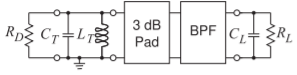
Figure \(\PageIndex{8}\)
- What is the oscillation frequency assuming that there is sufficient negative conductance for oscillation to occur?
- What is \(R_{D}\) when there is oscillation?
- A reflection oscillator is shown below along with the \(\Gamma_{r}\) and \(\Gamma_{d}\) loci plotted on a Smith chart. \(\Gamma_{r}\), the reflection coefficient looking into the resonator, rotates clockwise as frequency increases. \(\Gamma_{d}\), the reflection coefficient of the active device, is amplitude dependent but is frequency independent. The arrowed curve plots the loci of Γd as amplitude increases. [Hint: Consider Figure 5.5.4.]
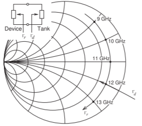
Figure \(\PageIndex{9}\)
- On the \(\Gamma_{r}\) plane show the region of the Smith Chart identifying oscillation.
- On the \(\Gamma_{d}\) plane show the region of the Smith Chart identifying oscillation.
- What is the frequency of oscillation?
- The case study presented in Section 5.6 described the design of a \(5\text{ GHz}\) VCO. The output of the oscillator was followed by a resistive Pi attenuator and then a bandpass filter. What is the attenuation (in decibels) and the system impedance of the attenuator. [Hint: You will need to carefully read Section 5.6.]
- Consider a common emitter BJT Clapp oscillator.
- Draw the schematic of the oscillator without the bias circuit.
- Redraw the oscillator circuit including the bias circuit.
- Consider a BJT Hartley oscillator.
- Draw the schematic of the oscillator circuit in the common-base configuration. Do not show the bias circuit.
- Redraw the schematic of the oscillator circuit in the common-base configuration, this time showing the bias circuit.
- Consider a FET Clapp oscillator.
- Draw the schematic of the oscillator circuit in the common drain configuration. Do not show the bias circuit.
- Redraw the schematic of the oscillator circuit, this time showing the bias circuit.
- Consider a FET Hartley oscillator.
- Draw the schematic of the oscillator circuit in the common source configuration. Do not show the bias circuit.
- Redraw the schematic of the oscillator circuit, this time showing the bias circuit.
- Consider a common source FET Clapp oscillator.
- Draw the schematic of the oscillator without biasing.
- Redraw the oscillator circuit including bias current sources.
- Derive an expression for the oscillation frequency of the Colpitts BJT oscillator in the common emitter configuration shown in Figure 5.8.1(b).
- A two-port feedback oscillator is shown in Figure 5.2.1.
- Draw the schematic of a feedback Colpitts oscillator.
- Considering that the amplifier in the feedback oscillator has a gain that is independent of frequency, what is the oscillation frequency if the components of the Colpitts feedback network are \(C_{1} = C_{2} = 2\text{ pF}\) and \(L_{3} = 5\text{ nH}\). Ignore any phase shift introduced by the amplifier.
- A two-port feedback oscillator is shown in Figure 5.2.1.
- Draw the schematic of a feedback Colpitts oscillator.
- Considering that the amplifier in the feedback oscillator has a gain that is independent of frequency, what is the oscillation frequency if the components of the Colpitts feedback network are \(C_{1} = 1\text{ pF},\: C_{2} = 3\text{ pF}\), and \(L_{3} = 1\text{ nH}\). Ignore any phase shift introduced by the amplifier.
- A two-port feedback oscillator is shown in Figure 5.2.1.
- Draw the schematic of a feedback Colpitts oscillator.
- Considering that the amplifier in the feedback oscillator has a gain that is independent of frequency, what is the oscillation frequency if the components of the Colpitts feedback network are \(C_{1} = 5\text{ pF},\: C_{2} = 1\text{ pF}\), and \(L_{3} = 10\text{ nH}\)? Ignore any phase shift introduced by the amplifier.
- A negative-gm differential FET VCO, as shown in Figure 5.7.1, has \(C = 0.2\text{ pF}\) and \(L = 0.2\text{ nH}\). \(V_{DD} = 5\text{ V}\) and the circuit is biased so that for each transistor \(g_{m} = 1\text{ mS}\). The output at the collector of the transistor drives a \(1\text{ k}\Omega\) load. Ignore the internal parasitics of the transistor and you must consider the possibility that the circuit does not oscillate. What is the oscillation frequency of the oscillator?
- A negative-gm differential FET VCO, as shown in Figure 5.7.1, has \(C = 0.2\text{ pF}\) and \(L = 0.2\text{ nH}\). \(V_{DD} = 5\text{ V}\) and the circuit is biased so that for each transistor \(g_{m} = 1\text{ mS}\). The output at the collector of the transistor drives a \(50\:\Omega\) differential load that is in parallel with a \(0.5\text{ pF}\) capacitor. Ignore the internal parasitics of the transistor and you must consider the possibility that the circuit does not oscillate.
- Draw the schematic of the oscillator with the load.
- Draw the equivalent tank circuit of the oscillator. This will need to include the effect of the load.
- What is the oscillation frequency of oscillator?
- A negative-gm differential FET VCO, as shown in Figure 5.7.1, has \(C = 0.2\text{ pF}\) and \(L = 0.2\text{ nH}\). \(V_{DD} = 5\text{ V}\) and the circuit is biased so that for each transistor \(g_{m} = 1\text{ mS}\). The output at the collector of the transistor drives a \(50\:\Omega\) differential load that is in parallel with a \(1\text{ pF}\) capacitor. Ignore the internal parasitics of the transistor and you must consider the possibility that the circuit does not oscillate. What is the oscillation frequency of the oscillator?
- A common emitter Colpitts oscillator, as shown in Figure 5.8.1(a), has \(C_{1} = 1\text{ pF}\), \(C_{2} = 2\text{ pF}\), and \(L_{3} = 2\text{ nH}\). \(L_{C}\) is a choke inductor. \(V_{CC} = 5\text{ V}\) and the circuit is biased so that \(g_{m} = 1\text{ mS}\). Ignore the internal parasitics of the transistor. What is the oscillation frequency of the oscillator? [Parallels Example 5.7.1]
- A common emitter Colpitts oscillator, as shown in Figure 5.8.1(a), has \(C_{1} = 0.1\text{ pF}\), \(C_{2} = 0.2\text{ pF}\), and \(L_{3} = 0.5\text{ nH}\). \(L_{C}\) is a choke inductor. \(V_{CC} = 5\text{ V}\) and the circuit is biased so that \(g_{m} = 1\text{ mS}\). Ignore the internal parasitics of the transistor. What is the oscillation frequency of the oscillator? [Parallels Example 5.7.1]
- A digital communication system has a symbol rate of \(1\text{ MS/s}\).
- What is the highest frequency phase noise that will affect the bit error rate of the communication system? (It could be \(1\text{ MHz}\), \(2\text{ MHZ}\), no limit, \(0.5\text{ MHz}\), etc.)
- What changes would you make to the system (e.g., added components such as an attenuator, filter, amplifier, etc.) that will reduce the impact of high-offset phase noise?
- A QPSK communication system has a transmitted bit rate of \(100\text{ kbit/s}\). Consider that the QPSK modulation scheme is ideal.
- What is the symbol rate?
- What would you do to the system (e.g., added components) to reduce the impact of high-offset phase noise?
- A QPSK communication system has a transmitted bit rate of \(1\text{ Mbit/s}\). The QPSK modulation scheme is ideal (\(2\text{ bit/s/Hz}\). DSP processing is such that phase noise slower than the duration of \(5\) symbols has no affect on the communication system throughput.
- What is the symbol rate?
- What is the lowest frequency phase noise that will affect the communication system?
- An oscillator has phase noise that reduces away from the oscillation center frequency, \(f_{\text{osc}}\) at the rate of \(1/\Delta f^{2}\) where \(\Delta f\) is the frequency offset from \(f_{\text{osc}}\). If the phase noise at \(100\text{ MHz}\) frequency offset from the oscillation frequency is \(−100\text{ dBc/Hz}\), what is the phase noise at \(10\text{ MHz}\)?
- The phase noise of an oscillator measured at \(1\text{ MHz}\) is \(−136\text{ dBc/Hz}\). If the phase noise varies as \(1/(\Delta f)\), where \(\Delta f\) is the offset from the center frequency of oscillation, what is the phase noise at \(100\text{ kHz}\) offset?
- A phase-locked microwave oscillator typically utilizes a low-\(Q\) oscillator. For such an oscillator the phase noise at the frequency that affects microwave systems has an inverse square relationship to frequency. The phase noise measured at \(100\text{ kHz}\) is \(−106\text{ dBc/Hz}\), what is the phase noise referred to \(1\text{ MHz}\)?
- A phase-locked microwave oscillator typically utilizes a low-\(Q\) oscillator. For such an oscillator the phase noise at the frequency that affects microwave systems often has an inverse square relationship to frequency. The phase noise measured at \(1\text{ MHz}\) is \(−125\text{ dBc/Hz}\), what is the phase noise at \(100\text{ kHz}\)?
5.12.1 Exercises by Section
\(†\)challenging, \(‡\)very challenging
\(§5.2\: 1\)
\(§5.3\: 2†, 3†, 4†, 5†, 6‡, 7‡, 8, 9, 10, 11\)
\(§5.5\: 12\)
\(§5.6\: 13†\)
\(§5.7\: 14†, 15†, 16†, 17†, 18†, 19†, 20†, 21†, 22†, 23†, 24†, 25†, 26†, 27†\)
\(§5.8\: 28†, 29†, 30†, 31, 32†, 33†, 34†\)
5.12.2 Answers to Selected Exercises
- \(4.594\text{ GHz}\)
- (d) \(49.8\:\Omega,\: 99.6\text{ fF}\)
- (e) \(4.883\text{ MHz}\)
- \(49.8\:\Omega,\: 2.97\text{ dB}\)
- \(\sqrt{\frac{C_{1}+C_{2}}{L_{3}C_{1}C_{2}}}\)
- \(1.592\text{ GHz}\)
- \(25.16\text{ GHz}\)
- (c) \(10.27\text{ GHz}\)
- \(100\text{ GHz}\)
- \(-105\text{ dBc/Hz}\)