
9.4: EXPERIMENTAL RESULTS
- Page ID
- 71816

\( \newcommand{\vecs}[1]{\overset { \scriptstyle \rightharpoonup} {\mathbf{#1}} } \)
\( \newcommand{\vecd}[1]{\overset{-\!-\!\rightharpoonup}{\vphantom{a}\smash {#1}}} \)
\( \newcommand{\id}{\mathrm{id}}\) \( \newcommand{\Span}{\mathrm{span}}\)
( \newcommand{\kernel}{\mathrm{null}\,}\) \( \newcommand{\range}{\mathrm{range}\,}\)
\( \newcommand{\RealPart}{\mathrm{Re}}\) \( \newcommand{\ImaginaryPart}{\mathrm{Im}}\)
\( \newcommand{\Argument}{\mathrm{Arg}}\) \( \newcommand{\norm}[1]{\| #1 \|}\)
\( \newcommand{\inner}[2]{\langle #1, #2 \rangle}\)
\( \newcommand{\Span}{\mathrm{span}}\)
\( \newcommand{\id}{\mathrm{id}}\)
\( \newcommand{\Span}{\mathrm{span}}\)
\( \newcommand{\kernel}{\mathrm{null}\,}\)
\( \newcommand{\range}{\mathrm{range}\,}\)
\( \newcommand{\RealPart}{\mathrm{Re}}\)
\( \newcommand{\ImaginaryPart}{\mathrm{Im}}\)
\( \newcommand{\Argument}{\mathrm{Arg}}\)
\( \newcommand{\norm}[1]{\| #1 \|}\)
\( \newcommand{\inner}[2]{\langle #1, #2 \rangle}\)
\( \newcommand{\Span}{\mathrm{span}}\) \( \newcommand{\AA}{\unicode[.8,0]{x212B}}\)
\( \newcommand{\vectorA}[1]{\vec{#1}} % arrow\)
\( \newcommand{\vectorAt}[1]{\vec{\text{#1}}} % arrow\)
\( \newcommand{\vectorB}[1]{\overset { \scriptstyle \rightharpoonup} {\mathbf{#1}} } \)
\( \newcommand{\vectorC}[1]{\textbf{#1}} \)
\( \newcommand{\vectorD}[1]{\overrightarrow{#1}} \)
\( \newcommand{\vectorDt}[1]{\overrightarrow{\text{#1}}} \)
\( \newcommand{\vectE}[1]{\overset{-\!-\!\rightharpoonup}{\vphantom{a}\smash{\mathbf {#1}}}} \)
\( \newcommand{\vecs}[1]{\overset { \scriptstyle \rightharpoonup} {\mathbf{#1}} } \)
\( \newcommand{\vecd}[1]{\overset{-\!-\!\rightharpoonup}{\vphantom{a}\smash {#1}}} \)
\(\newcommand{\avec}{\mathbf a}\) \(\newcommand{\bvec}{\mathbf b}\) \(\newcommand{\cvec}{\mathbf c}\) \(\newcommand{\dvec}{\mathbf d}\) \(\newcommand{\dtil}{\widetilde{\mathbf d}}\) \(\newcommand{\evec}{\mathbf e}\) \(\newcommand{\fvec}{\mathbf f}\) \(\newcommand{\nvec}{\mathbf n}\) \(\newcommand{\pvec}{\mathbf p}\) \(\newcommand{\qvec}{\mathbf q}\) \(\newcommand{\svec}{\mathbf s}\) \(\newcommand{\tvec}{\mathbf t}\) \(\newcommand{\uvec}{\mathbf u}\) \(\newcommand{\vvec}{\mathbf v}\) \(\newcommand{\wvec}{\mathbf w}\) \(\newcommand{\xvec}{\mathbf x}\) \(\newcommand{\yvec}{\mathbf y}\) \(\newcommand{\zvec}{\mathbf z}\) \(\newcommand{\rvec}{\mathbf r}\) \(\newcommand{\mvec}{\mathbf m}\) \(\newcommand{\zerovec}{\mathbf 0}\) \(\newcommand{\onevec}{\mathbf 1}\) \(\newcommand{\real}{\mathbb R}\) \(\newcommand{\twovec}[2]{\left[\begin{array}{r}#1 \\ #2 \end{array}\right]}\) \(\newcommand{\ctwovec}[2]{\left[\begin{array}{c}#1 \\ #2 \end{array}\right]}\) \(\newcommand{\threevec}[3]{\left[\begin{array}{r}#1 \\ #2 \\ #3 \end{array}\right]}\) \(\newcommand{\cthreevec}[3]{\left[\begin{array}{c}#1 \\ #2 \\ #3 \end{array}\right]}\) \(\newcommand{\fourvec}[4]{\left[\begin{array}{r}#1 \\ #2 \\ #3 \\ #4 \end{array}\right]}\) \(\newcommand{\cfourvec}[4]{\left[\begin{array}{c}#1 \\ #2 \\ #3 \\ #4 \end{array}\right]}\) \(\newcommand{\fivevec}[5]{\left[\begin{array}{r}#1 \\ #2 \\ #3 \\ #4 \\ #5 \\ \end{array}\right]}\) \(\newcommand{\cfivevec}[5]{\left[\begin{array}{c}#1 \\ #2 \\ #3 \\ #4 \\ #5 \\ \end{array}\right]}\) \(\newcommand{\mattwo}[4]{\left[\begin{array}{rr}#1 \amp #2 \\ #3 \amp #4 \\ \end{array}\right]}\) \(\newcommand{\laspan}[1]{\text{Span}\{#1\}}\) \(\newcommand{\bcal}{\cal B}\) \(\newcommand{\ccal}{\cal C}\) \(\newcommand{\scal}{\cal S}\) \(\newcommand{\wcal}{\cal W}\) \(\newcommand{\ecal}{\cal E}\) \(\newcommand{\coords}[2]{\left\{#1\right\}_{#2}}\) \(\newcommand{\gray}[1]{\color{gray}{#1}}\) \(\newcommand{\lgray}[1]{\color{lightgray}{#1}}\) \(\newcommand{\rank}{\operatorname{rank}}\) \(\newcommand{\row}{\text{Row}}\) \(\newcommand{\col}{\text{Col}}\) \(\renewcommand{\row}{\text{Row}}\) \(\newcommand{\nul}{\text{Nul}}\) \(\newcommand{\var}{\text{Var}}\) \(\newcommand{\corr}{\text{corr}}\) \(\newcommand{\len}[1]{\left|#1\right|}\) \(\newcommand{\bbar}{\overline{\bvec}}\) \(\newcommand{\bhat}{\widehat{\bvec}}\) \(\newcommand{\bperp}{\bvec^\perp}\) \(\newcommand{\xhat}{\widehat{\xvec}}\) \(\newcommand{\vhat}{\widehat{\vvec}}\) \(\newcommand{\uhat}{\widehat{\uvec}}\) \(\newcommand{\what}{\widehat{\wvec}}\) \(\newcommand{\Sighat}{\widehat{\Sigma}}\) \(\newcommand{\lt}{<}\) \(\newcommand{\gt}{>}\) \(\newcommand{\amp}{&}\) \(\definecolor{fillinmathshade}{gray}{0.9}\)While the amplifier described in this chapter was designed primarily as an educational vehicle, it has been built and tested, and can be used to demonstrate certain performance features of the two-stage design. Although a detailed description of the experimentally measured performance of this amplifier is of questionable value since it is not a commercially available design, the presentation of several transient responses seems a worthwhile prelude to the more detailed experimental evaluation of compensation included in Chapter 13.
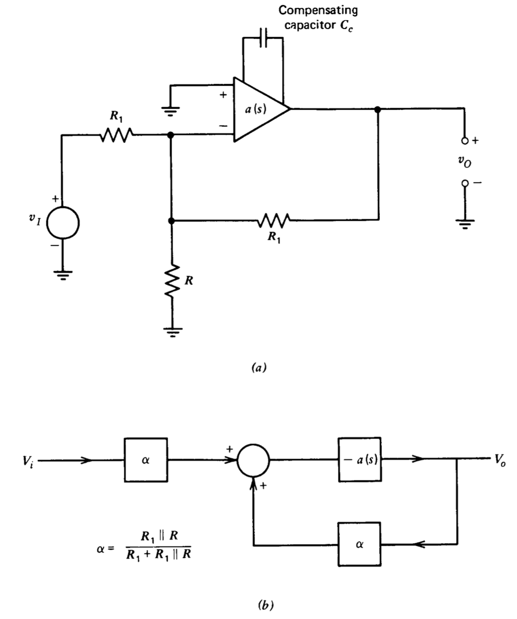
The amplifier was connected as shown in Figure 9.8\(a\). This connection, which results in the block diagram shown in Figure 9.8\(b\), is useful for demonstrations since it permits control of the loop transmission both by selection of the value of \(C_c\) [which influences \(a(s)\)] and by choice of \(R\). The ideal closed-loop gain of the connection is minus one independent of \(R\).
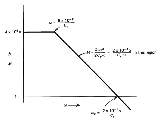
The magnitude of the loop transmission for this system, with only the lowest-frequency pole included, is shown in Bode-plot form in Figure 9.9. As anticipated, the crossover frequency is dependent on the ratio \(\alpha /C_c\).
The output of the amplifier in response to \(-20-mV\) step input signals with \(R = \infty\) (\(\alpha = 1/2\)) for four different values of compensating capacitor is shown in Figure 9.10. Note that for the larger values of \(C_c\), the response is very nearly first order, and that the 10 to 90% rise time agrees closely with the value predicted for single-pole systems, \(t_r = 2 .2 /\omega_c\). Smaller compen sating-capacitor values change the character of the response as the system becomes relatively less stable and faster. The highly oscillatory response that results for \(C_c = 5\ pF\) indicates that the phase shift added at the crossover frequency by the second- and higher-frequency poles is very nearly \(90^{\circ}\) in this case.
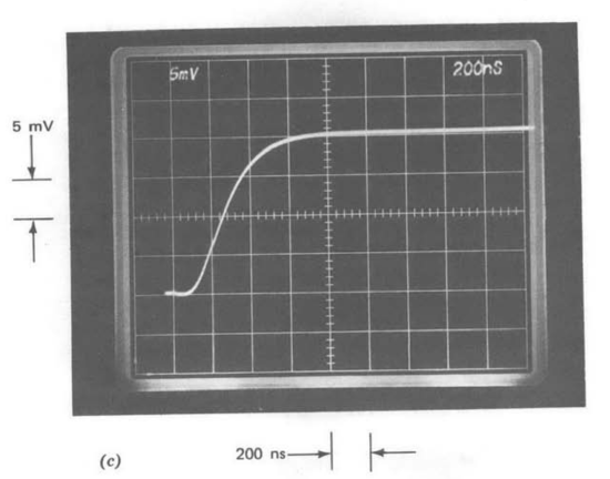
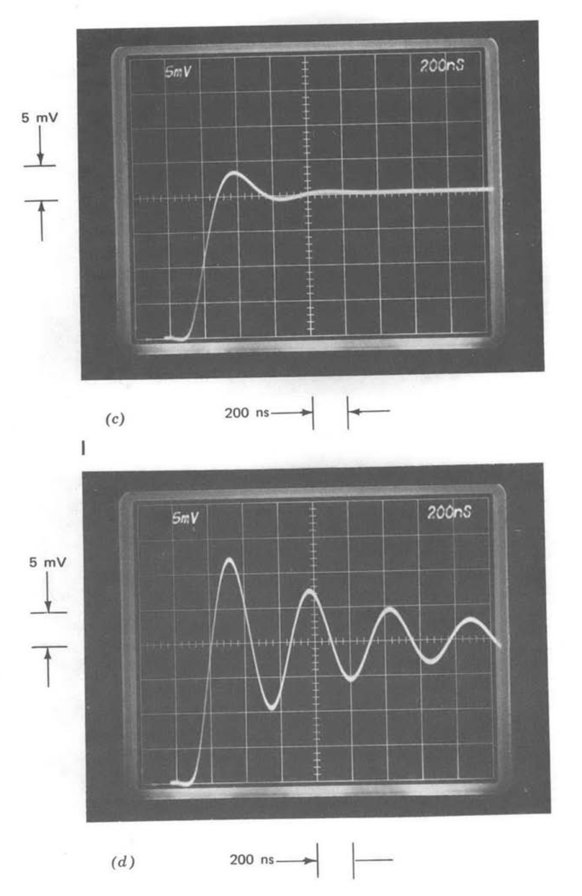
The step response shown in Figure 9.11 shows how this design allows the effects of changing attenuation inside the loop to be offset by altering compensation. While the attenuation is changed by changing the value of \(R\) in this demonstration, it depends on the ideal closed-loop gain in many practical connections. Figure 9.11\(a\) shows the step response for \(\alpha = 1/2\) (\(R = \infty\)) and \(C_c = 20\ pF\). The response for \(\alpha = 1/4\) (\(R = \tfrac{1}{2}R_1\)) and \(C_c = 20\ pF\) is shown in Figure 9.11\(b\). The rise time is approximately twice as long in Figure 9.11\(b\), anticipated since the crossover frequency is a factor of two lower in this connection (see Figure 9.9). The crossover frequency can be restored to its original value by lowering \(C_c\) to \(10\ pF\). The transient response for this value of compensating capacitor (Figure 9.11\(c\)) is virtually identical to that shown in part a of this figure.
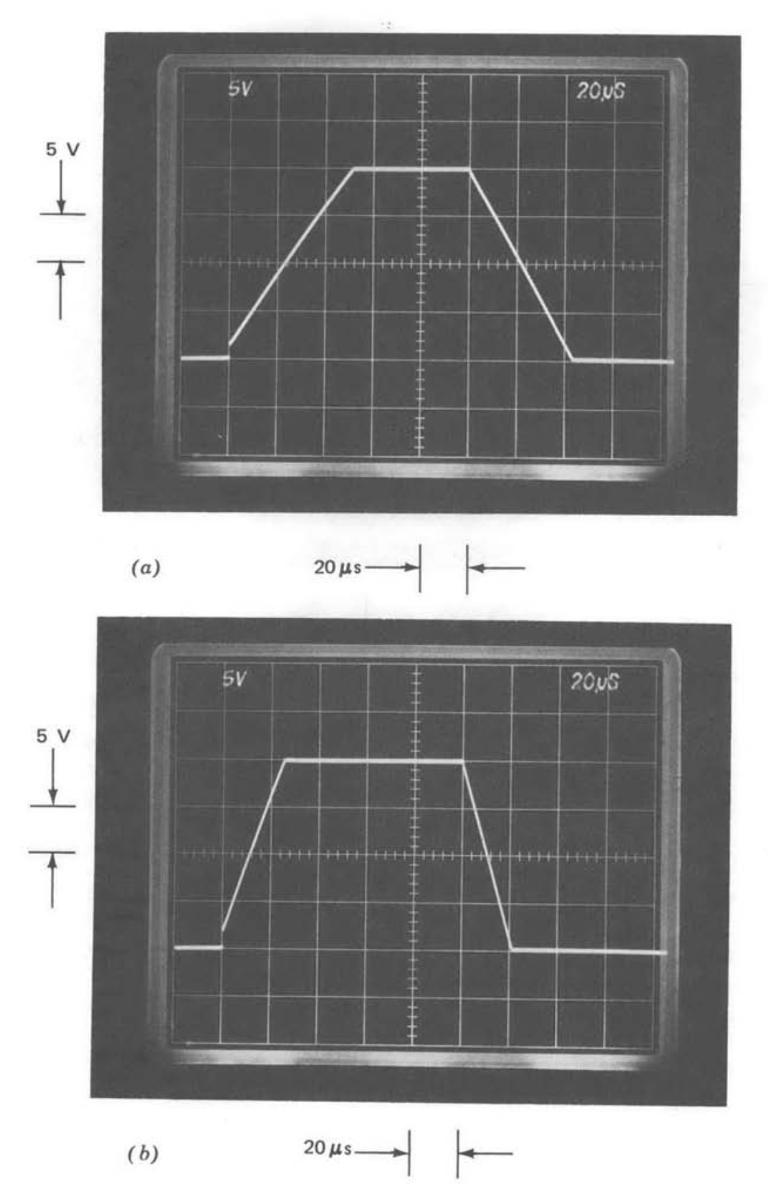
Figure 9.12 demonstrates the slew rate of the amplifier by showing its slew-rate limited response to \(20-\text{volt}\) peak-to-peak square wave signals. The parameter values for Figure 9.12\(a\) are \(\alpha = 1/2\) and \(C_c = 20\ pF\), while those of Figure 9.12\(b\) are \(\alpha = 1/4\) and \(C_c= 10\ pF\). These are the values that gave the virtually identical small-signal responses shown in Figs. 9.11\(a\) and 9.11\(c\), respectively. The large-signal responses show that the slew rate is inversely proportional to compensating-capacitor value, as predicted in Section 9.3.2.
PROBLEMS
Exercise \(\PageIndex{1}\)
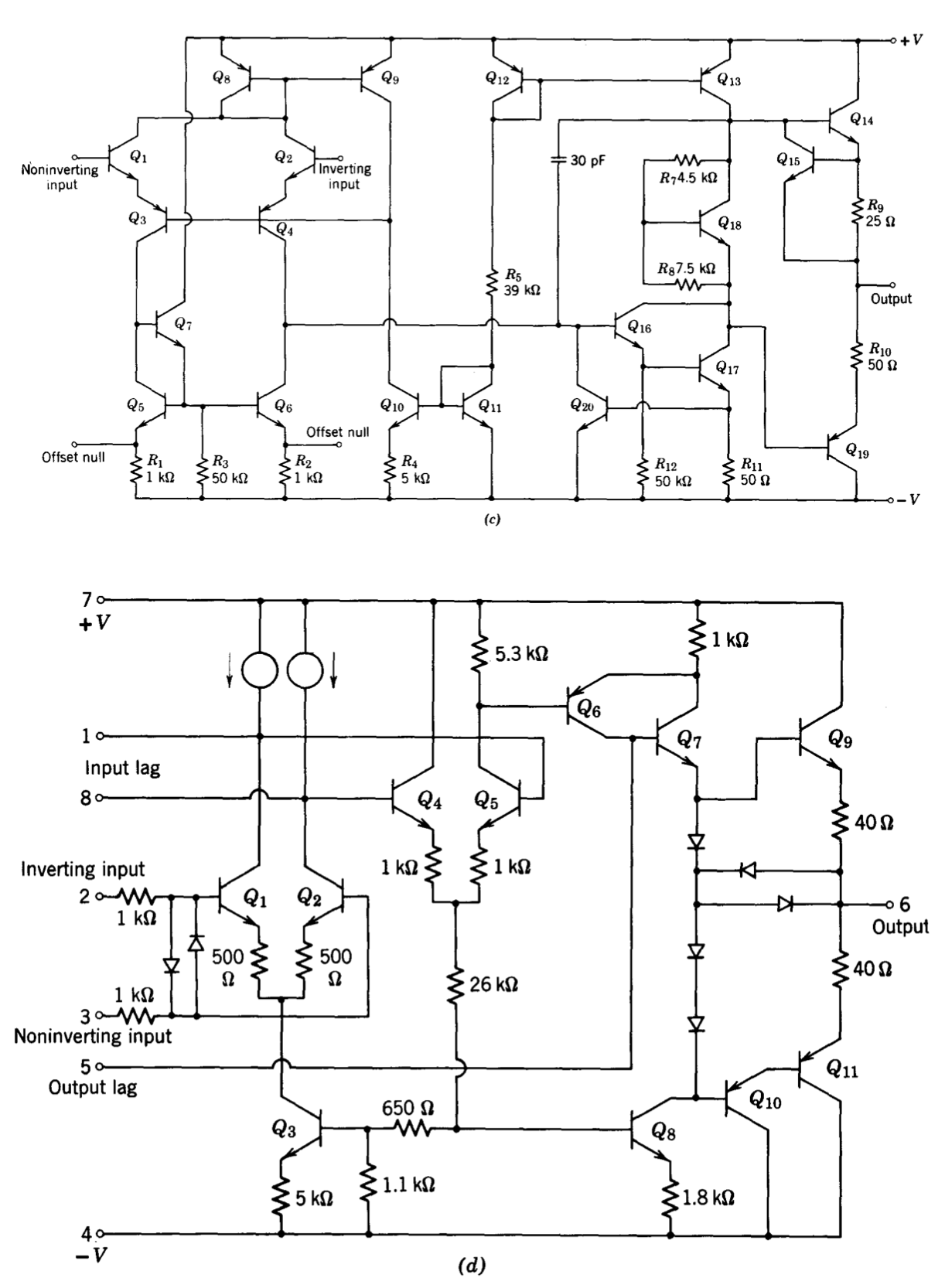
Figure 9.13 shows schematics for several available integrated circuits. Determine the transistors that actually contribute to signal amplification for each of these circuits.
Exercise \(\PageIndex{2}\)
Assume that measurements made on an operational amplifier of the type described in this chapter indicate a bias current required at either input terminal equal to \(9 \times 10^{-4}A/T^2\), where \(T\) is the temperature in degrees Kelvin. We intend to use the amplifier connected for a noninverting gain of two. Design a temperature-dependent network that can partially compensate the input current seen at the noninverting input of the amplifier. Note that since an input voltage range of \(\pm 5\) volts is anticipated, the incremental resistance of the compensating source must be the order of \(10^{10} \Omega\) to achieve good compensation.
Exercise \(\PageIndex{3}\)
The input transistors of the amplifier described in this chapter are matched such that the difference between the base-to-emitter voltages of these two devices is less than \(3\ mV\) when they operate at equal collector currents. Assume that this matching is not performed, and consequently that the base-to-emitter voltage of \(Q_2\) (see Figure 9.1) is \(50\ mV\) lower than that of \(Q_1\) when the two devices operate at equal currents. The amplifier can still be balanced by replacing the collector-circuit resistor network of the pair with a \(650-k\Omega\) potentiometer, and possibly changing the \(33-k\Omega\) resistor in the emitter circuit of the \(Q_4-Q_6\) pair so that the quiescent operating level of these devices remains \(50\ \mu A\) following balancing. Calculate the effect that balancing an amplifier with this degree of mismatch between input devices has on the open-loop gain of the amplifier.
Exercise \(\PageIndex{4}\)
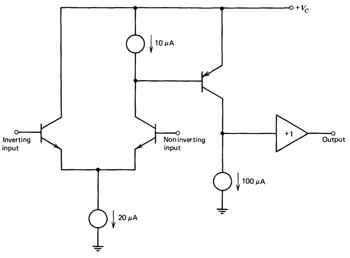
Figure 9.14 shows a simplified representation for an operational amplifier. You may assume that the current sources have infinite output impedance and that the buffer amplifier has infinite input resistance. All transistors are characterized by \(\beta = 200\) and \(\eta = 5 \times 10^{-4}\).
(a) Estimate the low-frequency open-loop gain of this configuration.
(b) What is the input offset voltage of the amplifier, assuming that the two input transistors have identical values for \(I_S\)?
(c) What is the common-mode rejection ratio of this amplifier?
(d) Estimate the time constant associated with the dominant amplifier pole, assuming all transistors have \(C_{\pi} = 10\ pF\), \(C_{\mu} = 5\ pF\).
(e) Suggest at least three circuit changes (aside from simply using better transistors) that can increase the value of the d-c open-loop gain.
Exercise \(\PageIndex{5}\)
An interesting amplifier topology that can be used for operational amplifiers intended to be connected as unity-gain voltage followers is shown in Figure 9.15. (Note that the amplifier is shown connected as a voltage follower.) You may assume that the current sources have infinite output impedance and that all transistors are characterized by \(\beta = 100\) and \(\eta = 2 \times 10^{-4}\).
(a) How many voltage-gain stages does this amplifier have?
(b) Estimate the unloaded, low-frequency open-loop gain of the amplifier.
(c) Estimate the low-frequency closed-loop output impedance of the circuit.
Exercise \(\PageIndex{6}\)
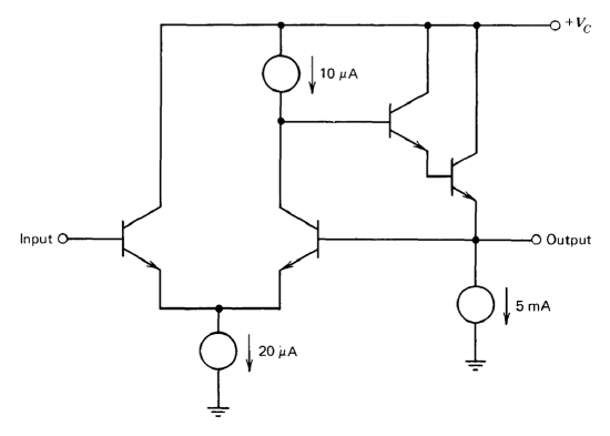
Assume that the field-effect transistor (\(Q_8\) in Figure 9.1) in the amplifier described in this chapter is replaced with a 2N3707. Use values given in Table 9.1, with appropriate modifications reflecting operation at \(2\ mA\), to determine values for \(g_m\), \(r_{\pi}\), \(r_o\), and \(r_{\mu}\).You may assume that the value of \(C_{\pi}\) at \(2\ mA\) is \(50\ pF\). Determine the changes in amplifier d-c open-loop gain and the changes in uncompensated dynamics that result from this design change.
Exercise \(\PageIndex{7}\)
A detailed analysis of a certain operational amplifier shows that its open-loop transfer function contains a single low-frequency pole, and that the location of this pole is easily controlled by appropriate compensation. In addition to this dominant pole, the open-loop transfer function includes 7 poles at \(s = - 10^8\text{ sec}^{-1}\) and two right-half-plane zeros at \(s = 2 \times 10^8\text{ sec}^{-1}\). Show that, at least at frequencies up to several megahertz, the net effect of these higher-frequency singularities can be modeled as a single time delay. Determine the delay time of an approximating transfer function. Use the time-delay approximation to describe the effect of the higher-order singularities on the maximum crossover frequency of feedback connections that include this amplifier inside the loop. If the d-c open-loop gain of the amplifier is \(10^5\), how should the dominant pole be located in order to achieve \(45^{\circ}\) of phase margin when the amplifier is connected as a unity-gain inverter?
Exercise \(\PageIndex{8}\)
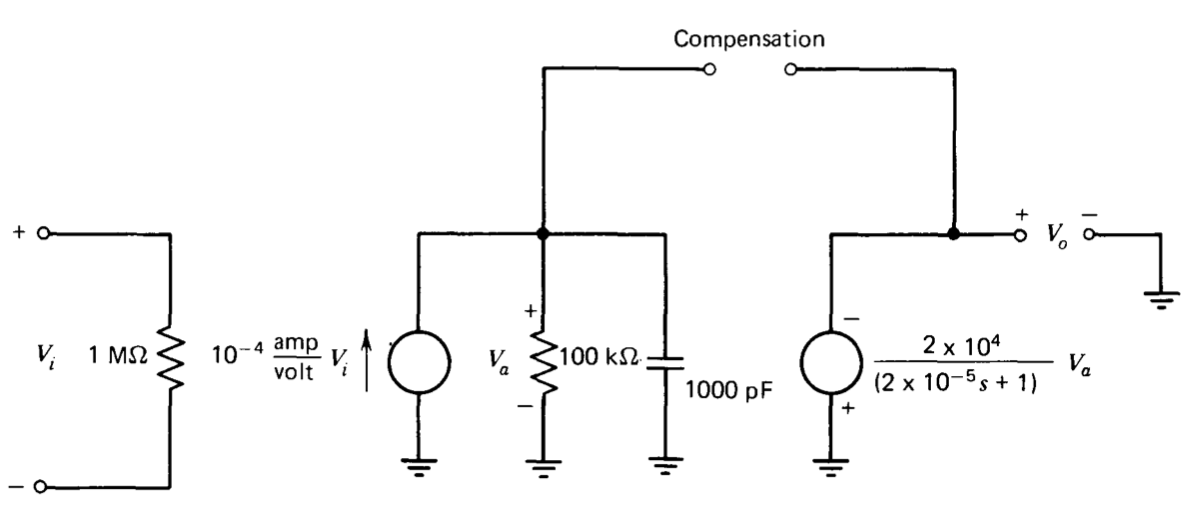
A model for an operational amplifier is shown in Figure 9.16. This amplifier is connected as a unity-gain voltage follower.
(a) What is the phase margin with no compensation?
(b) If a capacitor is used between the compensating terminals, how large a value is required to double the uncompensated phase margin?
(c) How large a capacitor should be used to obtain \(45^{\circ}\) of phase margin in the follower connection?
(d) An alternative compensating technique involves shunting a series \(R-C\) network across the \(100-k\Omega\) resistor and \(1000-pF\) capacitor combination shown in Figure 9.16. Find parameter values for this type of compensation that yields results similar to those obtained in part \(c\).
Exercise \(\PageIndex{9}\)
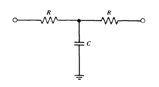
The amplifier described in Problem P9.8 is used in a loop where an approximate open-loop transfer function of \(10 (10^{-2} s + 1)\) is required. It is suggested that the required transfer function be obtained by compen sating the amplifier with the \(T\) network shown in Figure 9.17. Determine network-parameter values that might reasonably be expected to approxi mate the required transfer function.
When the amplifier is tested with this type of compensation, we find that our first guess was incorrect. Explain.
Exercise \(\PageIndex{10}\)
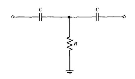
Another class of application involves the use of the \(T\) network shown in Figure 9.18 to compensate the amplifier described in Problem P9.8. This network can be used without encountering the type of difficulties that occur using the network described in Problem P9.9. Determine the type of transfer function that results using the high-pass \(T\), and comment on the value of this type of compensation.
Exercise \(\PageIndex{11}\)
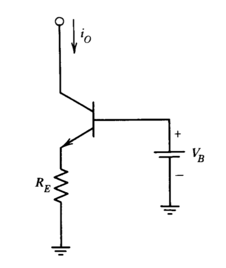
It was mentioned in Section 9.3.1 that the temperature stability of the amplifier described in this chapter could be improved by making the bias current source of the first stage have an output current directly proportional to temperature. This proportionality can be accomplished by means of the circuit shown in Figure 9.19. Assume that the transistor current-voltage characteristic is
\[i_C = AT^3 e^{eq(V_{BE} - V_{go})/kT}\nonumber \]
Determine the value of \(V_B\) that results in an output current directly proportional to temperature at \(300^{\circ} K\).
Exercise \(\PageIndex{12}\)
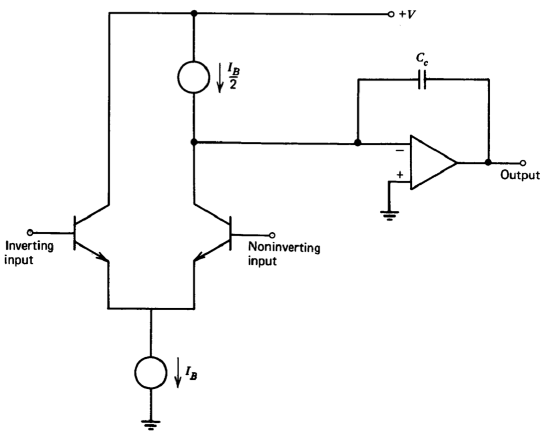
A two-stage operational amplifier can be modeled as shown in Figure 9.20. In this representation, the high-gain second stage itself is modeled as an operational amplifier with a minor-loop feedback element connected around it. You may assume that the second stage has ideal characteristics (i.e., infinite gain and input impedance, zero output impedance, etc.).
(a) Determine the unity-gain frequency of this amplifier as a function of \(I_B\) and \(C_c\).
(b) Express the slew rate of the amplifier in terms of the same parameters.
(c) Find a design modification that allows an increase in slew rate without increasing unity-gain frequency.