
7.2: Precision Rectifiers
- Page ID
- 3587

\( \newcommand{\vecs}[1]{\overset { \scriptstyle \rightharpoonup} {\mathbf{#1}} } \)
\( \newcommand{\vecd}[1]{\overset{-\!-\!\rightharpoonup}{\vphantom{a}\smash {#1}}} \)
\( \newcommand{\dsum}{\displaystyle\sum\limits} \)
\( \newcommand{\dint}{\displaystyle\int\limits} \)
\( \newcommand{\dlim}{\displaystyle\lim\limits} \)
\( \newcommand{\id}{\mathrm{id}}\) \( \newcommand{\Span}{\mathrm{span}}\)
( \newcommand{\kernel}{\mathrm{null}\,}\) \( \newcommand{\range}{\mathrm{range}\,}\)
\( \newcommand{\RealPart}{\mathrm{Re}}\) \( \newcommand{\ImaginaryPart}{\mathrm{Im}}\)
\( \newcommand{\Argument}{\mathrm{Arg}}\) \( \newcommand{\norm}[1]{\| #1 \|}\)
\( \newcommand{\inner}[2]{\langle #1, #2 \rangle}\)
\( \newcommand{\Span}{\mathrm{span}}\)
\( \newcommand{\id}{\mathrm{id}}\)
\( \newcommand{\Span}{\mathrm{span}}\)
\( \newcommand{\kernel}{\mathrm{null}\,}\)
\( \newcommand{\range}{\mathrm{range}\,}\)
\( \newcommand{\RealPart}{\mathrm{Re}}\)
\( \newcommand{\ImaginaryPart}{\mathrm{Im}}\)
\( \newcommand{\Argument}{\mathrm{Arg}}\)
\( \newcommand{\norm}[1]{\| #1 \|}\)
\( \newcommand{\inner}[2]{\langle #1, #2 \rangle}\)
\( \newcommand{\Span}{\mathrm{span}}\) \( \newcommand{\AA}{\unicode[.8,0]{x212B}}\)
\( \newcommand{\vectorA}[1]{\vec{#1}} % arrow\)
\( \newcommand{\vectorAt}[1]{\vec{\text{#1}}} % arrow\)
\( \newcommand{\vectorB}[1]{\overset { \scriptstyle \rightharpoonup} {\mathbf{#1}} } \)
\( \newcommand{\vectorC}[1]{\textbf{#1}} \)
\( \newcommand{\vectorD}[1]{\overrightarrow{#1}} \)
\( \newcommand{\vectorDt}[1]{\overrightarrow{\text{#1}}} \)
\( \newcommand{\vectE}[1]{\overset{-\!-\!\rightharpoonup}{\vphantom{a}\smash{\mathbf {#1}}}} \)
\( \newcommand{\vecs}[1]{\overset { \scriptstyle \rightharpoonup} {\mathbf{#1}} } \)
\(\newcommand{\longvect}{\overrightarrow}\)
\( \newcommand{\vecd}[1]{\overset{-\!-\!\rightharpoonup}{\vphantom{a}\smash {#1}}} \)
\(\newcommand{\avec}{\mathbf a}\) \(\newcommand{\bvec}{\mathbf b}\) \(\newcommand{\cvec}{\mathbf c}\) \(\newcommand{\dvec}{\mathbf d}\) \(\newcommand{\dtil}{\widetilde{\mathbf d}}\) \(\newcommand{\evec}{\mathbf e}\) \(\newcommand{\fvec}{\mathbf f}\) \(\newcommand{\nvec}{\mathbf n}\) \(\newcommand{\pvec}{\mathbf p}\) \(\newcommand{\qvec}{\mathbf q}\) \(\newcommand{\svec}{\mathbf s}\) \(\newcommand{\tvec}{\mathbf t}\) \(\newcommand{\uvec}{\mathbf u}\) \(\newcommand{\vvec}{\mathbf v}\) \(\newcommand{\wvec}{\mathbf w}\) \(\newcommand{\xvec}{\mathbf x}\) \(\newcommand{\yvec}{\mathbf y}\) \(\newcommand{\zvec}{\mathbf z}\) \(\newcommand{\rvec}{\mathbf r}\) \(\newcommand{\mvec}{\mathbf m}\) \(\newcommand{\zerovec}{\mathbf 0}\) \(\newcommand{\onevec}{\mathbf 1}\) \(\newcommand{\real}{\mathbb R}\) \(\newcommand{\twovec}[2]{\left[\begin{array}{r}#1 \\ #2 \end{array}\right]}\) \(\newcommand{\ctwovec}[2]{\left[\begin{array}{c}#1 \\ #2 \end{array}\right]}\) \(\newcommand{\threevec}[3]{\left[\begin{array}{r}#1 \\ #2 \\ #3 \end{array}\right]}\) \(\newcommand{\cthreevec}[3]{\left[\begin{array}{c}#1 \\ #2 \\ #3 \end{array}\right]}\) \(\newcommand{\fourvec}[4]{\left[\begin{array}{r}#1 \\ #2 \\ #3 \\ #4 \end{array}\right]}\) \(\newcommand{\cfourvec}[4]{\left[\begin{array}{c}#1 \\ #2 \\ #3 \\ #4 \end{array}\right]}\) \(\newcommand{\fivevec}[5]{\left[\begin{array}{r}#1 \\ #2 \\ #3 \\ #4 \\ #5 \\ \end{array}\right]}\) \(\newcommand{\cfivevec}[5]{\left[\begin{array}{c}#1 \\ #2 \\ #3 \\ #4 \\ #5 \\ \end{array}\right]}\) \(\newcommand{\mattwo}[4]{\left[\begin{array}{rr}#1 \amp #2 \\ #3 \amp #4 \\ \end{array}\right]}\) \(\newcommand{\laspan}[1]{\text{Span}\{#1\}}\) \(\newcommand{\bcal}{\cal B}\) \(\newcommand{\ccal}{\cal C}\) \(\newcommand{\scal}{\cal S}\) \(\newcommand{\wcal}{\cal W}\) \(\newcommand{\ecal}{\cal E}\) \(\newcommand{\coords}[2]{\left\{#1\right\}_{#2}}\) \(\newcommand{\gray}[1]{\color{gray}{#1}}\) \(\newcommand{\lgray}[1]{\color{lightgray}{#1}}\) \(\newcommand{\rank}{\operatorname{rank}}\) \(\newcommand{\row}{\text{Row}}\) \(\newcommand{\col}{\text{Col}}\) \(\renewcommand{\row}{\text{Row}}\) \(\newcommand{\nul}{\text{Nul}}\) \(\newcommand{\var}{\text{Var}}\) \(\newcommand{\corr}{\text{corr}}\) \(\newcommand{\len}[1]{\left|#1\right|}\) \(\newcommand{\bbar}{\overline{\bvec}}\) \(\newcommand{\bhat}{\widehat{\bvec}}\) \(\newcommand{\bperp}{\bvec^\perp}\) \(\newcommand{\xhat}{\widehat{\xvec}}\) \(\newcommand{\vhat}{\widehat{\vvec}}\) \(\newcommand{\uhat}{\widehat{\uvec}}\) \(\newcommand{\what}{\widehat{\wvec}}\) \(\newcommand{\Sighat}{\widehat{\Sigma}}\) \(\newcommand{\lt}{<}\) \(\newcommand{\gt}{>}\) \(\newcommand{\amp}{&}\) \(\definecolor{fillinmathshade}{gray}{0.9}\)Imagine for a moment that you would like to half-wave rectify the output of an oscillator. Probably the first thing that pops into your head is the use of a diode, as in Figure \(\PageIndex{1}\). As shown, the diode passes positive half waves and blocks negative half-waves. But, what happens if the input signal is only 0.5 V peak? Rectification never occurs because the diode requires 0.6 to 0.7 V to turn on. Even if a germanium device is used with a forward drop of 0.3 V, a sizable portion of the signal will be lost. Not only that, the circuit of Figure \(\PageIndex{1}\) exhibits vastly different impedances to the driving source. Even if the signal is large enough to avoid the forward voltage drop difficulty, the source impedance must be relatively low. At first glance it seems as though it is impossible to rectify a small AC signal with any hope of accuracy.
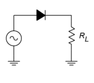
Figure \(\PageIndex{1}\): Passive rectifier.
One of the items noted in Chapter 3 about negative feedback was the fact that it tended to compensate for errors. Negative feedback tends to reduce errors by an amount equal to the loop gain. This being the case, it should be possible to reduce the diode's forward voltage drop by a very large factor by placing it inside of a feedback loop. This is shown in Figure \(\PageIndex{2}\), and is called a precision half-wave rectifier.
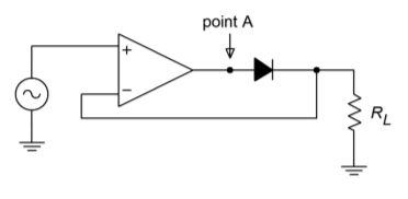
Figure \(\PageIndex{2}\): Precision half-wave rectifier.
To a first approximation, when the input is positive, the diode is forward-biased. In essence, the circuit reduces to a simple voltage follower with a high input impedance and a voltage gain of one, so the output looks just like the input. On the other hand, when the input is negative, the diode is reverse-biased, opening up the feedback loop. No signal current is allowed to the load, so the output voltage is zero. Thanks to the op amp, though, the driving source still sees a high impedance. The output waveform consists of just the positive portions of the input signal, as shown in Figure \(\PageIndex{3}\). Due to the effect of negative feedback, even small signals may be properly rectified. The resulting transfer characteristic is presented in Figure \(\PageIndex{4}\). A perfect one-to-one input/output curve is seen for positive input signals, whereas negative input signals produce an output potential of zero.
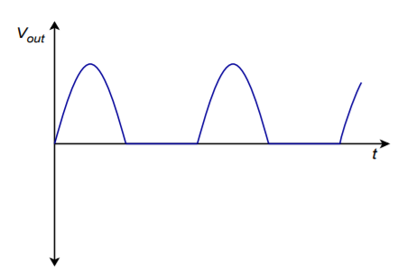
Figure \(\PageIndex{3}\): Output signal.
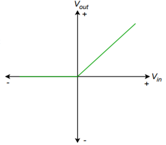
Figure \(\PageIndex{4}\): Transfer characteristic.
In order to create the circuit output waveform, the op amp creates an entirely different waveform at its output pin. For positive portions of the input, the op amp must produce a signal that is approximately 0.6 to 0.7 V greater than the final circuit output. This extra signal effectively compensates for the diode's forward drop. Because the feedback signal is derived after the diode, the compensation is as close as the available loop gain allows. At low frequencies where the loop gain is high, the compensation is almost exact, producing a near perfect copy of positive signals. When the input signal swings negative, the op amp tries to sink current in response. As it does so, the diode becomes reverse-biased, and current flow is halted. At this point the op amp's noninverting input will see a large negative potential relative to the inverting input. The resulting negative error signal forces the op amp's output to go to negative saturation. Because the diode remains reverse-biased, the circuit output stays at 0 V. The op amp is no longer able to drive the load. This condition will persist until the input signal goes positive again, at which point the error signal becomes positive, forward-biasing the diode and allowing load current to flow. The op amp and circuit output waveforms are shown in Figure \(\PageIndex{5}\).
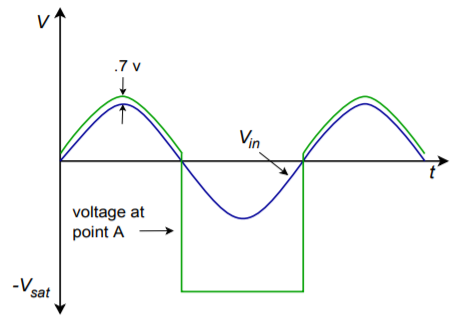
Figure \(\PageIndex{5}\): Output of op amp.
One item to note about Figure \(\PageIndex{5}\) is the amount of time it takes for the op amp to swing in and out of negative saturation. This time is determined by the device's slew rate. Along with the decrease of loop gain at higher frequencies, slew rate determines how accurate the rectification will be. Suppose that the op amp is in negative saturation and that a quick positive input pulse occurs. In order to track this, the op amp must climb out of negative saturation first. Using a 741 op amp with \(\pm\)15 V supplies, it will take about 26 \(\mu\)s to go from negative saturation (-13 V) to zero. If the aforementioned pulse is only 20 \(\mu\)s wide, the circuit doesn't have enough time to produce the pulse. The input pulse will have gone negative again, before the op amp has a chance to “climb out of its hole”. If the positive pulse were a bit longer, say 50 \(\mu\)s, the op amp would be able to track a portion of it. The result would be a distorted signal as shown in Figure \(\PageIndex{6}\).
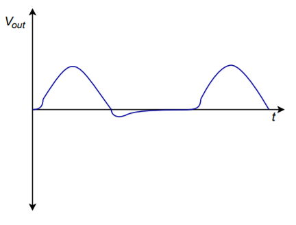
Figure \(\PageIndex{6}\): High frequency errors.
In order to accurately rectify fast moving signals, op amps with high \(f_{unity}\) and slew rate are required. If only slow signals are to be rectified, it is possible to configure the circuit with moderate gain if needed, as a cost-saving measure. This is shown in Figure \(\PageIndex{7}\). Finally, for negative half-wave output, the only modification required is the reversal of the diode.
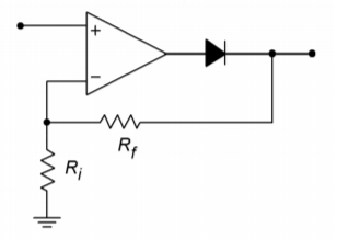
Figure \(\PageIndex{7}\): Rectifier with gain.
Computer Simulation
A Multisim simulation of the circuit shown in Figure \(\PageIndex{2}\) is presented in Figure 7.8. The circuit is shown redrawn with the nodes labeled. This example utilizes the 741 op amp model examined earlier. The output waveform is also shown in Figure \(\PageIndex{8}\). Note the accuracy of the rectification. The output of the op amp is also shown so that the effects of negative feedback illustrated in \(\PageIndex{5}\) are clearly visible. Because this circuit utilizes an accurate op amp model, it is very instructive to rerun the simulation for higher input frequencies. In this way, the inherent speed limitations of the op amp are shown, and effects such as those presented in Figure \(\PageIndex{6}\) may be noted.
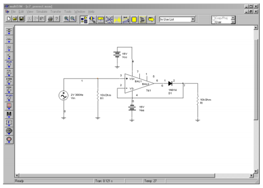
Figure \(\PageIndex{8a}\): Precision rectifier simulation schematic.
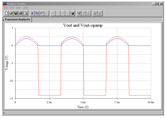
Figure \(\PageIndex{8b}\): Output waveforms of precision rectifier.
7.2.1: Peak Detector
One variation on the basic half-wave rectifier is the peak detector. This circuit will produce an output that is equal to the peak value of the input signal. This can be configured for either positive or negative peaks. The output of a peak detector can be used for instrumentation or measurement applications. It can also be thought of as an analog pulse stretcher.
A simple positive peak detector is shown in Figure \(\PageIndex{9}\). Here is how it works: The first portion of the circuit is a precision positive half-wave rectifier. When its output is rising, the capacitor, \(C\), is being charged. This voltage is presented to the second op amp that serves as a buffer for the final load. The output impedance of the first op amp is low, so the charge time constant is very fast, and thus the signal across \(C\) is very close to the input signal. When the input signal starts to swing back toward ground, the output of the first op amp starts to drop along with it. Due to the capacitor voltage, the diode ends up in reverse-bias, thus opening the drive to \(C\). \(C\) starts to discharge, but the discharge time constant will be much longer than the charge time constant. The discharge resistance is a function of \(R\), the impedance looking into the noninverting input of op amp 2, and the impedance looking into the inverting input of op amp 1, all in parallel. Normally, FET input devices are used, so from a practical standpoint, \(R\) sets the discharge rate.
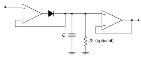
Figure \(\PageIndex{9}\): Peak detector.
The capacitor will continue to discharge toward zero until the input signal rises enough to overtake it again. If the discharge time constant is much longer than the input period, the circuit output will be a DC value equal to the peak value of the input. If the discharge time constant is somewhat shorter, it has the effect of lengthening the pulse time. It also has the effect of producing the overall contour, or envelope, of complex signals, so it is sometimes called an envelope detector. Possible output signals are shown in Figure \(\PageIndex{10}\). For very long discharge times, large capacitors must be used. Larger capacitors will, of course, produce a lengthening of the charge time (i.e., the rise time will suffer). Large capacitors can also degrade slewing performance. \(C\) can only be charged so fast because a given op amp can only produce a finite current. This is no different than the case presented with compensation capacitors back in Chapter Five. As an example, if C is 10 \(\mu\)F, and the maximum output current of the op amp is 25 mA,
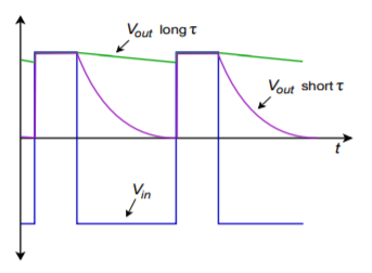
Figure \(\PageIndex{10}\): Effect of \(\tau\) on pulse shape.
\[ i = C \frac{dv}{dt} \nonumber \]
\[ \frac{dv}{dt} = \frac{i}{C} \nonumber \]
\[ \frac{dv}{dt} = \frac{25 mA}{10 \mu F} \nonumber \]
\[ \frac{dv}{dt} = 2500 V/s \nonumber \]
\[ \frac{dv}{dt} = 2.5 mV/\mu s \nonumber \]
This is a very slow slew rate! If FET input devices are used, the effective discharge resistance can be very high, thus lowering the requirement for \(C\). For typical applications, \(C\) would be many times smaller than the value used here. For long discharge times, high quality capacitors must be used, as their internal leakage will place the upper limit on discharge resistance.
Example \(\PageIndex{1}\)
A positive peak detector is used along with a simple comparator in Figure \(\PageIndex{11}\) to monitor input levels and warn of possible overload. The LF412 is a dual-package version of the LF411. Explain how it works and determine the point at which the LED lights.
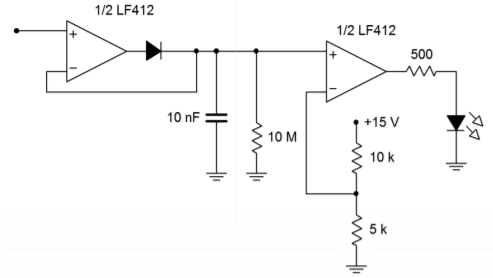
Figure \(\PageIndex{11}\): Detector for Example \(\PageIndex{1}\).
The basic problem when trying to visually monitor a signal for overloads is that the overloading peak may come and go faster than the human eye can detect it. For example, the signal might be sent to a comparator that could light an LED when a preset threshold is exceeded. When the input signal falls, the comparator and LED will go into the off state. Even though the LED does light at the peak, it remains on for such a short time that humans won't notice it. This sort of result is quite possible in the communications industry, where the output of a radio station's microphone will produce very dynamic waves with a great many peaks. These peaks can cause havoc in other pieces of equipment down the line. The LED needs to remain on for longer periods.
The circuit of Figure \(\PageIndex{11}\) uses a peak detector to stretch out the positive pulses. These stretched pulses are then fed to a comparator, which drives an LED. The input pulses are expanded, so the LED will remain on for longer periods.
The discharge time constant is set by \(R\) and \(C\). Because FET input devices are used, their impedance is high enough to ignore.
\[ T = RC \nonumber \]
\[ T = 10 M \Omega \times 10 nF \nonumber \]
\[ T = 100 ms \nonumber \]
The 10 nF capacitor is small enough to maintain a reasonable slew rate. You may wish to verify this as an exercise. The comparator trip point is set by the 10 k\(\Omega\)/5 k\(\Omega\) voltage divider at 5 V. When the input signal rises above 5 V, the comparator output goes high. Assuming that the LED forward drop is about 2.5 V, the 500 \(\Omega\) resistor limits the output current to
\[ I_{LED} = \frac{V_{sat} − V_{LED}}{500} \nonumber \]
\[ I_{LED} = \frac{13 V−2.5 V}{500} \nonumber \]
\[ I_{LED} = \frac{10.5 V}{500} \nonumber \]
\[ I_{LED} = 21 mA \nonumber \]
The LF412 should be able to deliver this current.
In summary, then, the input pulses are stretched by the peak detector. If any of the resulting pulses are greater than 5 V, the comparator trips, and lights the LED. An example input/output wave is shown in Figure \(\PageIndex{12}\). The one problem with this is that only positive peaks are detected. If large negative peaks exist, they will not cause the LED to light. It is possible to use a similar circuit to detect negative peaks and use that output to drive a common LED along with the positive peak detector. Another way to accomplish this is to utilize a full-wave rectifier/detector.
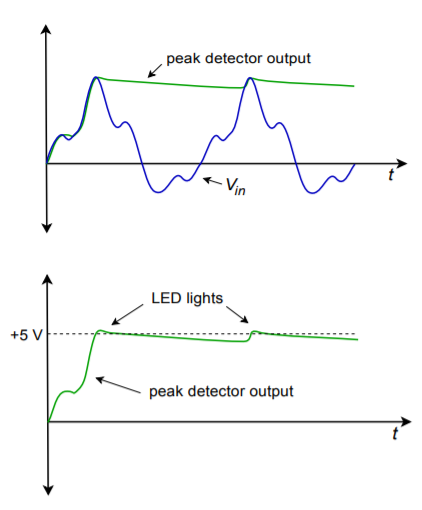
Figure \(\PageIndex{12}\): Waveforms for the circuit of Figure \(\PageIndex{11}\).
7.2.2: Precision Full-Wave Rectifier
A full-wave rectifier has the input/output characteristic shown in Figure \(\PageIndex{13}\). No matter what the input polarity is, the output is always positive. For this reason, this circuit is often referred to as an absolute value circuit. The design of a precision full-wave rectifier is a little more involved than the single-polarity types. One way of achieving this design is to combine the outputs of negative and positive half-wave circuits with a differential amplifier. Another way is shown in Figure \(\PageIndex{14}\).
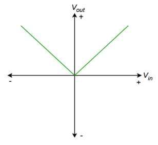
Figure \(\PageIndex{13}\): Transfer characteristic for fullwave rectification.
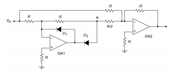
Figure \(\PageIndex{14}\): Precision full-wave rectifier.
The precision rectifier of circuit \(\PageIndex{14}\) is convenient in that it only requires two op amps and that all resistors (save one) are the same value. This circuit is comprised of two parts: an inverting half-wave rectifier and a weighted summing amplifier. The rectifier portion is redrawn in Figure \(\PageIndex{15}\). Let's start the analysis with this portion.
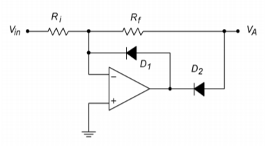
Figure \(\PageIndex{15}\): Inverting half-wave rectifier.
First, note that the circuit is based on an inverting voltage amplifier, with the diodes \(D_1\) and \(D_2\) added. For positive input signals, the input current will attempt to flow through \(R_f\), to create an inverted output signal with a gain of \(R_f/R_i\). (Normally, gain is set to unity.) Because the op amp's inverting input is more positive than its noninverting input, the op amp tries to sink output current. This forces \(D_2\) on, completing the feedback loop, while also forcing \(D_1\) off. As \(D_2\) is inside the feedback loop, its forward drop is compensated for. Thus, positive input signals are amplified and inverted as in a normal inverting amplifier.
If the input signal is negative, the op amp will try to source current. This turns \(D_1\) on, creating a path for current flow. Because the inverting input is at virtual ground, the output voltage of the op amp is limited to the 0.6 to 0.7 V drop of \(D_1\). In this way, the op amp does not saturate; rather, it delivers the current required to satisfy the source demand. The op amp's output polarity also forces \(D_2\) off, leaving the circuit output at an approximate ground. Therefore, for negative input signals, the circuit output is zero. The combination of the positive and negative input swings creates an inverted, half-wave rectified output signal, as shown in Figure \(\PageIndex{16}\). This circuit can be used on its own as a half-wave rectifier if need be. Its major drawback is a somewhat limited input impedance. On the plus side, because the circuit is non-saturating, it may prove to be faster than the half-wave rectifier first discussed.
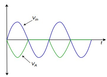
Figure \(\PageIndex{16}\): Output of half-wave rectifier.
The voltage at point A in Figure \(\PageIndex{14}\) is the output of the half-wave rectifier as shown in Figure \(\PageIndex{16}\). This is one of two signals applied to the summer configured around op amp 2. The other input to the summer is the main circuit's input signal. This signal is given a gain of unity, and the half-wave signal is given a gain of two. These two signals will combine as shown in Figure \(\PageIndex{17}\) to create a positive full-wave output. Mathematically,
For the first 180 degrees:
\[ V_{out} =−K \sin \omega t+2 K \sin \omega t \nonumber \]
\[ V_{out} = K \sin \omega t \nonumber \]
For the second 180 degrees:
\[ V_{out} = K \sin \omega t+0 \nonumber \]
\[ V_{out} = K \sin \omega t \nonumber \]
In order to produce a negative full-wave rectifier, simply reverse the polarity of \(D_1\) and \(D_2\).
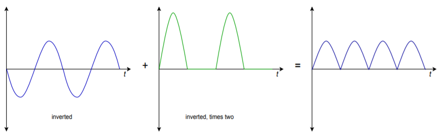
Figure \(\PageIndex{17}\): Combination of signals produces output.
An example application of an op amp-based rectifier is shown in Figure \(\PageIndex{18}\). This circuit is used detect dangerous overloads and faults in an audio power amplifier. Short-term signal clipping may not be a severe problem in certain applications; however, long-term clipping may create very stressful conditions for the loudspeakers. This would also be the case if an improperly functioning power amplifier produced a DC offset. Unfortunately, a simple scaled comparison of the input and output signals of the power amplifier may be misleading. In order to compare long-term averages, the input and scaled output signals are precision full-wave rectified and then passed through a peak-detecting or averaging stage. This might be as simple as a single RC network. These signals are then compared by the fault stage. If there is a substantial difference between the two signals, the amplifier is most likely clipping the signal considerably or producing an unwanted DC offset. The fault stage can then light a warning LED, or in severe cases, trip system shutdown circuitry to prevent damage to other components.
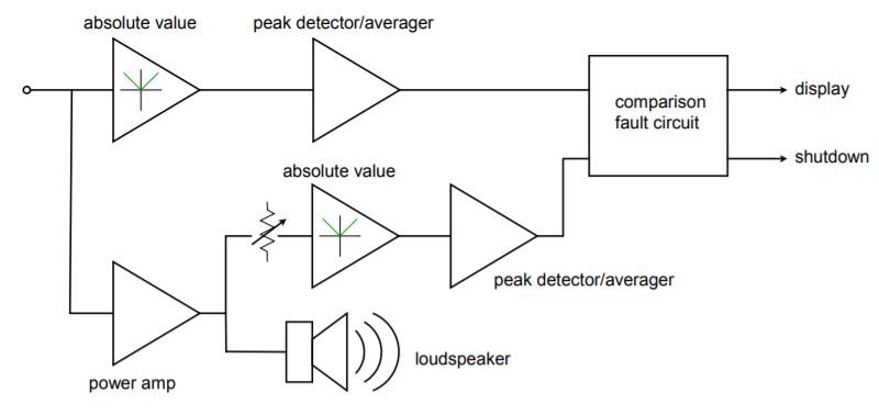
Figure \(\PageIndex{18}\): Power amplifier overload detector.