
2.4: Diode Circuit Models
- Page ID
- 25385

\( \newcommand{\vecs}[1]{\overset { \scriptstyle \rightharpoonup} {\mathbf{#1}} } \)
\( \newcommand{\vecd}[1]{\overset{-\!-\!\rightharpoonup}{\vphantom{a}\smash {#1}}} \)
\( \newcommand{\dsum}{\displaystyle\sum\limits} \)
\( \newcommand{\dint}{\displaystyle\int\limits} \)
\( \newcommand{\dlim}{\displaystyle\lim\limits} \)
\( \newcommand{\id}{\mathrm{id}}\) \( \newcommand{\Span}{\mathrm{span}}\)
( \newcommand{\kernel}{\mathrm{null}\,}\) \( \newcommand{\range}{\mathrm{range}\,}\)
\( \newcommand{\RealPart}{\mathrm{Re}}\) \( \newcommand{\ImaginaryPart}{\mathrm{Im}}\)
\( \newcommand{\Argument}{\mathrm{Arg}}\) \( \newcommand{\norm}[1]{\| #1 \|}\)
\( \newcommand{\inner}[2]{\langle #1, #2 \rangle}\)
\( \newcommand{\Span}{\mathrm{span}}\)
\( \newcommand{\id}{\mathrm{id}}\)
\( \newcommand{\Span}{\mathrm{span}}\)
\( \newcommand{\kernel}{\mathrm{null}\,}\)
\( \newcommand{\range}{\mathrm{range}\,}\)
\( \newcommand{\RealPart}{\mathrm{Re}}\)
\( \newcommand{\ImaginaryPart}{\mathrm{Im}}\)
\( \newcommand{\Argument}{\mathrm{Arg}}\)
\( \newcommand{\norm}[1]{\| #1 \|}\)
\( \newcommand{\inner}[2]{\langle #1, #2 \rangle}\)
\( \newcommand{\Span}{\mathrm{span}}\) \( \newcommand{\AA}{\unicode[.8,0]{x212B}}\)
\( \newcommand{\vectorA}[1]{\vec{#1}} % arrow\)
\( \newcommand{\vectorAt}[1]{\vec{\text{#1}}} % arrow\)
\( \newcommand{\vectorB}[1]{\overset { \scriptstyle \rightharpoonup} {\mathbf{#1}} } \)
\( \newcommand{\vectorC}[1]{\textbf{#1}} \)
\( \newcommand{\vectorD}[1]{\overrightarrow{#1}} \)
\( \newcommand{\vectorDt}[1]{\overrightarrow{\text{#1}}} \)
\( \newcommand{\vectE}[1]{\overset{-\!-\!\rightharpoonup}{\vphantom{a}\smash{\mathbf {#1}}}} \)
\( \newcommand{\vecs}[1]{\overset { \scriptstyle \rightharpoonup} {\mathbf{#1}} } \)
\(\newcommand{\longvect}{\overrightarrow}\)
\( \newcommand{\vecd}[1]{\overset{-\!-\!\rightharpoonup}{\vphantom{a}\smash {#1}}} \)
\(\newcommand{\avec}{\mathbf a}\) \(\newcommand{\bvec}{\mathbf b}\) \(\newcommand{\cvec}{\mathbf c}\) \(\newcommand{\dvec}{\mathbf d}\) \(\newcommand{\dtil}{\widetilde{\mathbf d}}\) \(\newcommand{\evec}{\mathbf e}\) \(\newcommand{\fvec}{\mathbf f}\) \(\newcommand{\nvec}{\mathbf n}\) \(\newcommand{\pvec}{\mathbf p}\) \(\newcommand{\qvec}{\mathbf q}\) \(\newcommand{\svec}{\mathbf s}\) \(\newcommand{\tvec}{\mathbf t}\) \(\newcommand{\uvec}{\mathbf u}\) \(\newcommand{\vvec}{\mathbf v}\) \(\newcommand{\wvec}{\mathbf w}\) \(\newcommand{\xvec}{\mathbf x}\) \(\newcommand{\yvec}{\mathbf y}\) \(\newcommand{\zvec}{\mathbf z}\) \(\newcommand{\rvec}{\mathbf r}\) \(\newcommand{\mvec}{\mathbf m}\) \(\newcommand{\zerovec}{\mathbf 0}\) \(\newcommand{\onevec}{\mathbf 1}\) \(\newcommand{\real}{\mathbb R}\) \(\newcommand{\twovec}[2]{\left[\begin{array}{r}#1 \\ #2 \end{array}\right]}\) \(\newcommand{\ctwovec}[2]{\left[\begin{array}{c}#1 \\ #2 \end{array}\right]}\) \(\newcommand{\threevec}[3]{\left[\begin{array}{r}#1 \\ #2 \\ #3 \end{array}\right]}\) \(\newcommand{\cthreevec}[3]{\left[\begin{array}{c}#1 \\ #2 \\ #3 \end{array}\right]}\) \(\newcommand{\fourvec}[4]{\left[\begin{array}{r}#1 \\ #2 \\ #3 \\ #4 \end{array}\right]}\) \(\newcommand{\cfourvec}[4]{\left[\begin{array}{c}#1 \\ #2 \\ #3 \\ #4 \end{array}\right]}\) \(\newcommand{\fivevec}[5]{\left[\begin{array}{r}#1 \\ #2 \\ #3 \\ #4 \\ #5 \\ \end{array}\right]}\) \(\newcommand{\cfivevec}[5]{\left[\begin{array}{c}#1 \\ #2 \\ #3 \\ #4 \\ #5 \\ \end{array}\right]}\) \(\newcommand{\mattwo}[4]{\left[\begin{array}{rr}#1 \amp #2 \\ #3 \amp #4 \\ \end{array}\right]}\) \(\newcommand{\laspan}[1]{\text{Span}\{#1\}}\) \(\newcommand{\bcal}{\cal B}\) \(\newcommand{\ccal}{\cal C}\) \(\newcommand{\scal}{\cal S}\) \(\newcommand{\wcal}{\cal W}\) \(\newcommand{\ecal}{\cal E}\) \(\newcommand{\coords}[2]{\left\{#1\right\}_{#2}}\) \(\newcommand{\gray}[1]{\color{gray}{#1}}\) \(\newcommand{\lgray}[1]{\color{lightgray}{#1}}\) \(\newcommand{\rank}{\operatorname{rank}}\) \(\newcommand{\row}{\text{Row}}\) \(\newcommand{\col}{\text{Col}}\) \(\renewcommand{\row}{\text{Row}}\) \(\newcommand{\nul}{\text{Nul}}\) \(\newcommand{\var}{\text{Var}}\) \(\newcommand{\corr}{\text{corr}}\) \(\newcommand{\len}[1]{\left|#1\right|}\) \(\newcommand{\bbar}{\overline{\bvec}}\) \(\newcommand{\bhat}{\widehat{\bvec}}\) \(\newcommand{\bperp}{\bvec^\perp}\) \(\newcommand{\xhat}{\widehat{\xvec}}\) \(\newcommand{\vhat}{\widehat{\vvec}}\) \(\newcommand{\uhat}{\widehat{\uvec}}\) \(\newcommand{\what}{\widehat{\wvec}}\) \(\newcommand{\Sighat}{\widehat{\Sigma}}\) \(\newcommand{\lt}{<}\) \(\newcommand{\gt}{>}\) \(\newcommand{\amp}{&}\) \(\definecolor{fillinmathshade}{gray}{0.9}\)One thing is very clear from the characteristic curve of the diode: It is not a linear bilateral1 device, quite unlike a resistor. Consequently, we cannot use the superposition technique to solve diode circuits unless we have a priori knowledge about it, that is, whether or not it is forward- or reverse-biased. For example, we can imagine a circuit comprised of two voltage sources, resistors and a diode. By itself, one of the voltage sources might forward-bias the diode while the other would reverse-bias it. Obviously, a diode cannot be both forward and reverse-biased at the same time.
A second problem we face with circuit analysis is the added complexity of the Shockley equation. For speed and ease of computation we find it useful to model the diode with simpler circuit elements. Three diode models are shown in Figure \(\PageIndex{1}\).
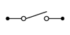
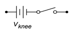
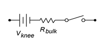
Figure \(\PageIndex{1}\): Simplified diode models. Top to bottom: first, second and third approximations, increasing in accuracy.
The first approximation is the simplest of the three. It treats the diode as a simple dependent switch: the switch is closed if the diode is forward-biased and open if it is reverse-biased. The second approximation adds the effect of the forward voltage. \(V_{knee}\) is the “turn-on” potential required to overcome the energy hill. It would be 0.7 volts for a silicon device. The third approximation is the most accurate of the three. A close look at the characteristic curve of Figure 2.2.4 shows that once the knee voltage is reached, the curve does not transition to a perfect vertical line. Instead, there remains some positive, non-infinite slope. That is, the voltage continues to increase, although modestly, with further increases in current. We can approximate this effect as a small resistive value, \(R_{bulk}\). The three corresponding I-V plots are shown in Figure \(\PageIndex{2}\). Compare these to Figure 2.2.6 and note the increasing accuracy.
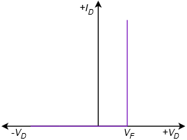
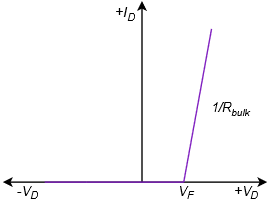
Figure \(\PageIndex{2}\): I-V curves for simplified diode models. Top to bottom: first, second and third approximations.
In many applications the second approximation will yield sufficiently accurate results and we will tend to make greatest use of it. Just remember that these are behavioral models; don't think that there are literally 0.7 volt sources or little resistors in the diodes.
It should be noted that \(R_{bulk}\) does not represent the “diode resistance” per se, rather, it models a minimum value. There really is no such thing as a singular diode resistance. We can, however, talk about the effective resistance of a diode in a particular circuit in both DC and AC terms.
The key to understanding this concept is to remember that resistance is a linear function, a straight line on a I-V graph. Therefore, we need to find a straight line “fit” for the diode curve. Two possibilities are shown in Figure \(\PageIndex{3}\).
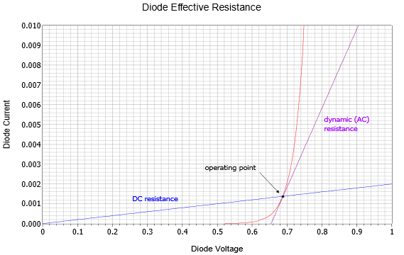
Figure \(\PageIndex{3}\): Diode effective resistance for DC and AC.
The red curve is the diode's characteristic curve (arbitrary current values are shown). For some particular DC circuit, a specific current will flow through the diode which will produce a particular voltage, denoted on the graph as the operating point. If we simply compute the ratio of that voltage to the driving current, we wind up with a resistance. This is the effective DC resistance of the diode under these circuit conditions and is represented by the blue line. That is, the reciprocal of the slope of the blue line is the effective DC resistance. Obviously, if we shift the operating point along the red diode curve, the slope of the intersecting blue line changes and therefore we arrive at a new DC resistance. The higher the current, the lower the effective DC resistance.
Instead of just DC, the diode might see a combination of DC and AC signals. Visualize this as adding a small AC variation on top of the DC. We can imagine the operating point moving along the red diode curve, back and forth about the operating point. If we divide the small AC voltage variation by its associated AC current variation, we wind up with the AC equivalent resistance, also known as the dynamic resistance. Graphically, we can think of this as finding the slope of a line that is tangent to the operating point (the purple line). This will in fact, be an average value across the AC variation. It should also be apparent that the effective AC resistance must be smaller than its DC counterpart because the AC approximation (purple line) must be steeper than the DC approximation (blue line)2. It is time for a few illustrative examples.
Example \(\PageIndex{1}\)
Consider the resistor-diode circuit of Figure \(\PageIndex{4}\). Assume the voltage source is 12 volts and the resistor is 2 k\(\Omega\). Further, assume the diode is silicon and its bulk resistance is 10 \(\Omega\). Using the three diode approximations, compute the circulating current.
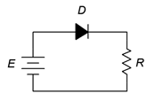
Figure \(\PageIndex{4}\): Schematic for Example \(\PageIndex{1}\).
First, note that the diode is forward-biased. This must be the case because there is a single voltage that is larger than the knee voltage and its positive terminal is attached to the diode's anode. No matter which approximation we use, Kirchhoff's voltage law (KVL) must be true so it will be a matter of summing the available voltage drops versus resistance(s).
Using the first approximation:
Here we assume the diode is a closed switch. Consequently all of the source voltage must drop across the single resistor.
\[I = \frac{E}{R} \nonumber \]
\[I = \frac{12V}{2 k\Omega} \nonumber \]
\[I = 6mA \nonumber \]
Using the second approximation:
In this instance we include the knee voltage.
\[I = \frac{E−V_{knee}}{R} \nonumber \]
\[I = \frac{ 12 V−0.7 V}{2 k\Omega} \nonumber \]
\[I = 5.65mA \nonumber \]
Using the third approximation:
The most accurate of the three, we include both the knee voltage and bulk resistance.
\[I = \frac{ E−V_{knee}}{R+R_{bulk}} \nonumber \]
\[I = \frac{ 12 V−0.7 V}{2 k\Omega+10 \Omega} \nonumber \]
\[I = 5.622mA \nonumber \]
In this particular case the difference between the second and third approximations is less than 1%. It is also worth noting that the third approximation predicts a diode voltage of slightly more than 0.7 volts (approximately 0.756 volts) due to the additional potential across the bulk resistance.
Example \(\PageIndex{2}\)
Determine the circulating current for the circuit in Figure \(\PageIndex{5}\). Also find the diode and resistor voltages. Assume the power supply is 20 volts, the diode is silicon and the resistor is 2 k\(\Omega\).
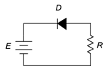
Figure \(\PageIndex{5}\): Schematic for Example \(\PageIndex{2}\).
This problem is deceptively easy. Note that the positive terminal of the source is connected to the cathode. As there are no other sources in the circuit, the diode must be reverse-biased. The model for a reverse-biased diode is an open switch and the circulating current in an open circuit is zero. Therefore, the resistor voltage must also be zero and values for the knee voltage and bulk resistance are not needed. In order to satisfy KVL, the diode voltage will equal the source of 20 volts (+ to − from cathode to anode).
The only time this would not be the case is if the reverse breakdown voltage of the diode is less than the 20 volt source. In that case the diode voltage would equal the breakdown voltage with the remainder of the source voltage dropping across the resistor.
Example \(\PageIndex{3}\)
Determine the circulating current for the circuit in Figure \(\PageIndex{6}\). Also find the diode and resistor voltages. Assume the power supply is 9 volts, the diodes are silicon and \(R_1\) = 1 k\(\Omega\), \(R_2\) = 2 k\(\Omega\).
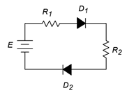
Figure \(\PageIndex{6}\): Schematic for Example \(\PageIndex{3}\).
According to KVL, the applied source must equal the sum of the voltage drops across the resistors and diodes as this is a single loop. Both diodes are forward-biased (conventional current entering the anodes).
\[I = \frac{ E−V_{knee1} − V_{knee2}}{R_1+R_2} \nonumber \]
\[I = \frac{ 9V−0.7V−0.7V}{1k \Omega +2 k\Omega} \nonumber \]
\[I = 2.533mA \nonumber \]
Note that if either diode was reversed, there would be no current flow and all of the source potential would drop across the reversed diode.
Example \(\PageIndex{4}\)
Determine the source current and resistor voltages for the circuit in Figure \(\PageIndex{7}\). Also find the resistor voltages if the diode polarity is reversed. Assume the power supply is 10 volts, the diode is silicon and the resistors are 1 k\(\Omega\) each.
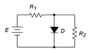
Figure \(\PageIndex{7}\): Schematic for Example \(\PageIndex{4}\).
As \(D\) and \(R_2\) are in parallel they must have the same voltage drop. Also, the diode is forward-biased. Therefore, the voltage across \(R_2\) must be approximately 0.7 volts, leaving 9.3 volts to drop across \(R_1\). The current through \(R_1\) is the source current.
\[I = \frac{E−V_D}{R_1} \nonumber \]
\[I = \frac{10 V−0.7 V}{1k \Omega} \nonumber \]
\[I = 9.3mA \nonumber \]
If the diode is reversed it behaves as an open switch. The circuit reduces to a simple 1:1 voltage divider, each resistor dropping half of the supply, or 5 volts each.
Computer Simulation
To verify our results, Example \(\PageIndex{4}\) is simulated. The circuit is captured as shown in Figure \(\PageIndex{8a}\). This particular example is shown in Multisim although any decent quality simulator will do. The very common 1N4148 switching diode is used here. Another popular choice would be the 1N914 switching diode or a 1N400X series rectifier.
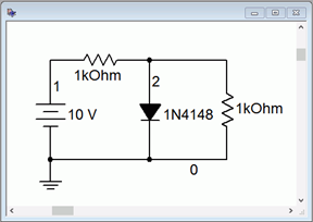
Figure \(\PageIndex{8a}\): The circuit of Example \(\PageIndex{4}\) in Multisim.
Next, a DC Operating Point analysis is performed. The results are shown in Figure \(\PageIndex{8b}\). Note that the diode potential is just under the 0.7 volt approximation. From this we can deduce that the voltage drop across the first resistor must be slightly more than 9.3 volts, producing a current slightly more than 9.3 mA.
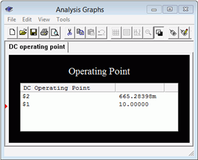
Figure \(\PageIndex{8b}\): DC Operating Point simulation results for the circuit of Example \(\PageIndex{4}\).
Finally, Figure \(\PageIndex{8c}\) shows the results when the diode is reversed in the circuit. The second resistor (node 3 to ground) shows 5 volts as expected. Therefore, the first resistor must also be dropping 5 volts.
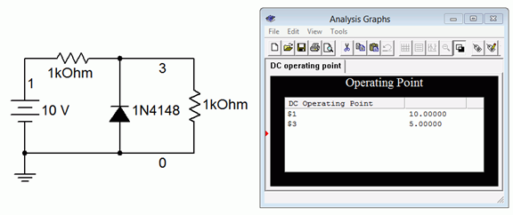
Figure \(\PageIndex{8c}\): Simulation of Example \(\PageIndex{4}\) using reversed diode orientation.
Before moving on to another topic, let's take a look at a somewhat more involved example using multiple diodes.
Example \(\PageIndex{5}\)
Determine the diode and resistor voltages for the circuit in Figure \(\PageIndex{9}\). Assume the diodes are silicon.
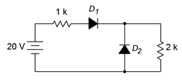
Figure \(\PageIndex{9}\): Schematic for Example \(\PageIndex{5}\).
The first thing to notice is that \(D_1\) is forward-biased while \(D_2\) is reverse-biased. Therefore, the 20 volt source must equal the drop across \(D_1\) and the two resistors. \(D_2\) will take on whatever the drop across the 2 k\(\Omega\) works out to as they are in parallel.
\[I = \frac{E−V_{D1}}{R_1+R_2} \nonumber \]
\[I = \frac{20 V−0.7V}{1k\Omega +2 k\Omega} \nonumber \]
\[I = 6.433mA \nonumber \]
Note that virtually no current flows down through \(D_2\) as it is reverse-biased. Using Ohm's law, the drop across the first resistor is 6.433 volts and for the second resistor, 12.867 volts.
References
1The I-V plot is not a straight line (linear) and the forward and reverse quadrants are not identical (bilateral).
2The dynamic resistance of a PN junction may be approximated as 26 mV/\(I_{junction}\). This will be shown in an upcoming chapter.