

9.5: Exercises
- Page ID
- 25442

\( \newcommand{\vecs}[1]{\overset { \scriptstyle \rightharpoonup} {\mathbf{#1}} } \)
\( \newcommand{\vecd}[1]{\overset{-\!-\!\rightharpoonup}{\vphantom{a}\smash {#1}}} \)
\( \newcommand{\dsum}{\displaystyle\sum\limits} \)
\( \newcommand{\dint}{\displaystyle\int\limits} \)
\( \newcommand{\dlim}{\displaystyle\lim\limits} \)
\( \newcommand{\id}{\mathrm{id}}\) \( \newcommand{\Span}{\mathrm{span}}\)
( \newcommand{\kernel}{\mathrm{null}\,}\) \( \newcommand{\range}{\mathrm{range}\,}\)
\( \newcommand{\RealPart}{\mathrm{Re}}\) \( \newcommand{\ImaginaryPart}{\mathrm{Im}}\)
\( \newcommand{\Argument}{\mathrm{Arg}}\) \( \newcommand{\norm}[1]{\| #1 \|}\)
\( \newcommand{\inner}[2]{\langle #1, #2 \rangle}\)
\( \newcommand{\Span}{\mathrm{span}}\)
\( \newcommand{\id}{\mathrm{id}}\)
\( \newcommand{\Span}{\mathrm{span}}\)
\( \newcommand{\kernel}{\mathrm{null}\,}\)
\( \newcommand{\range}{\mathrm{range}\,}\)
\( \newcommand{\RealPart}{\mathrm{Re}}\)
\( \newcommand{\ImaginaryPart}{\mathrm{Im}}\)
\( \newcommand{\Argument}{\mathrm{Arg}}\)
\( \newcommand{\norm}[1]{\| #1 \|}\)
\( \newcommand{\inner}[2]{\langle #1, #2 \rangle}\)
\( \newcommand{\Span}{\mathrm{span}}\) \( \newcommand{\AA}{\unicode[.8,0]{x212B}}\)
\( \newcommand{\vectorA}[1]{\vec{#1}} % arrow\)
\( \newcommand{\vectorAt}[1]{\vec{\text{#1}}} % arrow\)
\( \newcommand{\vectorB}[1]{\overset { \scriptstyle \rightharpoonup} {\mathbf{#1}} } \)
\( \newcommand{\vectorC}[1]{\textbf{#1}} \)
\( \newcommand{\vectorD}[1]{\overrightarrow{#1}} \)
\( \newcommand{\vectorDt}[1]{\overrightarrow{\text{#1}}} \)
\( \newcommand{\vectE}[1]{\overset{-\!-\!\rightharpoonup}{\vphantom{a}\smash{\mathbf {#1}}}} \)
\( \newcommand{\vecs}[1]{\overset { \scriptstyle \rightharpoonup} {\mathbf{#1}} } \)
\(\newcommand{\longvect}{\overrightarrow}\)
\( \newcommand{\vecd}[1]{\overset{-\!-\!\rightharpoonup}{\vphantom{a}\smash {#1}}} \)
\(\newcommand{\ket}[1]{\left| #1 \right>}\)
\(\newcommand{\bra}[1]{\left< #1 \right|}\)
\(\newcommand{\braket}[2]{\left< #1 \vphantom{#2} \right| \left. #2 \vphantom{#1} \right>}\)
\(\newcommand{\braopket}[3]{\left< #1 \vphantom{#2}\vphantom{#3} \right| #2 \vphantom{#1}\vphantom{#3} \left| #3 \vphantom{#1}\vphantom{#2} \right>}\)
\(\newcommand{\qmvec}[1]{\mathbf{\vec{#1}}}\)
\(\newcommand{\op}[1]{\hat{\mathbf{#1}}}\)
\(\newcommand{\expect}[1]{\langle #1 \rangle}\)
\(\newcommand{\dfn}[1]{\emph{\textbf{#1}}}\)
9.5.1: Analysis Problems
1. For the circuit of Figure \(\PageIndex{1}\), determine compliance, \(P_{load(max)}\), \(P_{D(max)}\), \(BV_{CEO}\) and \(I_{C(max)}\). \(V_{CC}\) = 15 V, \(V_{EE}\) = −15 V, \(\beta\) = 75, \(R_L\) = 16 \(\Omega\), \(R_1\) = 680 \(\Omega\), \(R_2\) = 680 \(\Omega\).
2. For the circuit of Figure \(\PageIndex{1}\), determine \(Z_{in}\). \(V_{CC}\) = 15 V, \(V_{EE}\) = −15 V, \(\beta\) = 75, \(R_L\) = 16 \(\Omega\), \(R_1\) = 680 \(\Omega\), \(R_2\) = 680 \(\Omega\).
3. For the circuit of Figure \(\PageIndex{1}\), determine \(Z_{in}\). \(V_{CC}\) = 25 V, \(V_{EE}\) = −25 V, \(\beta\) = 70, \(R_L\) = 8 \(\Omega\), \(R_1\) = 560 \(\Omega\), \(R_2\) = 560 \(\Omega\).
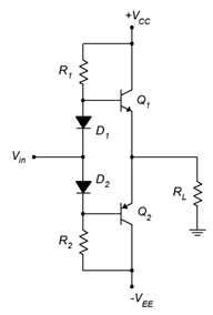
Figure \(\PageIndex{1}\)
4. For the circuit of Figure \(\PageIndex{1}\), determine compliance \(P_{load(max)}\), \(P_{D(max)}\), \(BV_{CEO}\) and \(I_{C(max)}\). \(V_{CC}\) = 25 V, \(V_{EE}\) = −25 V, \(\beta\) = 70, \(R_L\) = 8 \(\Omega\), \(R_1\) = 560 \(\Omega\), \(R_2\) = 560 \(\Omega\).
5. For the circuit of Figure \(\PageIndex{2}\), determine \(P_{load(max)}\), \(P_{D(max)}\), \(BV_{CEO}\) and \(I_{C(max)}\). \(V_{CC}\) = 15 V, \(\beta\) = 75, \(R_L\) = 16 \(\Omega\), \(R_1\) = 630 \(\Omega\), \(R_2\) = 630 \(\Omega\).
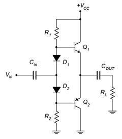
Figure \(\PageIndex{2}\)
6. For the circuit of Figure \(\PageIndex{2}\), determine \(Z_{in}\). \(V_{CC}\) = 15 V, \(\beta\) = 75, \(R_L\) = 16 \(\Omega\), \(R_1\) = 630 \(\Omega\), \(R_2\) = 630 \(\Omega\).
7. For the circuit of Figure \(\PageIndex{2}\), determine \(Z_{in}\). \(V_{CC}\) = 25 V, \(\beta\) = 70, \(R_L\) = 8 \(\Omega\), \(R_1\) = 560 \(\Omega\), \(R_2\) = 560 \(\Omega\).
8. For the circuit of Figure \(\PageIndex{2}\), determine \(P_{load(max)}\), \(P_{D(max)}\), \(BV_{CEO}\) and \(I_{C(max)}\). \(V_{CC}\) = 25 V, \(\beta\) = 70, \(R_L\) = 8 \(\Omega\), \(R_1\) = 510 \(\Omega\), \(R_2\) = 510 \(\Omega\).
9. For the circuit of Figure \(\PageIndex{3}\), determine \(P_{load(max)}\), \(P_{D(max)}\), \(BV_{CEO}\) and \(I_{C(max)}\) for the output transistors. \(V_{CC}\) = 24 V, \(V_{EE}\) = −24 V, \(\beta\) = 75, \(R_L\) = 8 \(\Omega\), \(R_1\) = 2.5 k\(\Omega\), \(R_2\) = 300 \(\Omega\), \(R_3\) = 330 \(\Omega\), \(R_4\) = 63 \(\Omega\).
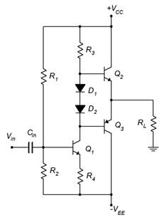
Figure \(\PageIndex{3}\)
10. For the circuit of Figure \(\PageIndex{3}\), determine \(A_v\) and \(Z_{in}\). \(V_{CC}\) = 24 V, \(V_{EE}\) = −24 V, \(\beta\) = 75, \(R_L\) = 8 \(\Omega\), \(R_1\) = 2.5 k\(\Omega\), \(R_2\) = 300 \(\Omega\), \(R_3\) = 330 \(\Omega\), \(R_4\) = 63 \(\Omega\).
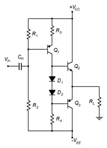
Figure \(\PageIndex{4}\)
11. For the circuit of Figure \(\PageIndex{4}\), determine \(P_{load(max)}\), \(P_{D(max)}\), \(BV_{CEO}\) and \(I_{C(max)}\) for the output transistors. \(V_{CC}\) = 24 V, \(V_{EE}\) = −24 V, \(\beta\) = 75, \(R_L\) = 16 \(\Omega\), \(R_1\) = 600 \(\Omega\), \(R_2\) = 5 k\(\Omega\), \(R_3\) = 63 \(\Omega\), \(R_4\) = 330 \(\Omega\).
12. For the circuit of Figure \(\PageIndex{4}\), determine \(A_v\) and \(Z_{in}\). \(V_{CC}\) = 24 V, \(V_{EE}\) = −24 V, \(\beta\) = 75, \(R_L\) = 16 \(\Omega\), \(R_1\) = 600 \(\Omega\), \(R_2\) = 5 k\(\Omega\), \(R_3\) = 63 \(\Omega\), \(R_4\) = 330 \(\Omega\).
13. Determine the limit current for the circuit of Figure \(\PageIndex{5}\) if \(R_E\) = 0.2 \(\Omega\).
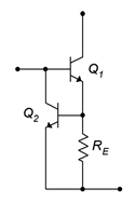
Figure \(\PageIndex{5}\)
14. Determine \(P_{load(max)}\), and \(P_{D(max)}\), \(BV_{CEO}\) and \(I_{C(max)}\) for the output and driver transistors of Figure \(\PageIndex{6}\). \(V_{CC}\) = 50 V, \(V_{EE}\) = −50 V, \(\beta\) = 75, \(R_L\) = 8 \(\Omega\), \(R_5\) through \(R_8\) = 0.05 \(\Omega\). Assume all other components produce proper bias.
9.5.2: Design Problems
15. For the circuit of Figure \(\PageIndex{3}\), determine values for \(R_1\) and \(R_2\) for proper bias. \(V_{CC}\) = 32 V, \(V_{EE}\) = −32 V, \(\beta\) = 75, \(R_L\) = 8 \(\Omega\), \(R_3\) = 330 \(\Omega\), \(R_4\) = 63 \(\Omega\).
16. Determine a value for \(R_E\) to set the limit current for the circuit of Figure \(\PageIndex{5}\) to 2 A.
9.5.3: Challenge Problems
17. For the circuit of Figure \(\PageIndex{6}\), determine values for \(R_1\) and \(R_2\) for proper bias. \(V_{CC}\) = 50 V, \(V_{EE}\) = −50 V, \(\beta\) = 85, \(R_L\) = 8 \(\Omega\), \(R_5\) through \(R_8\) = 0.05 \(\Omega\), \(R_3\) = 2.2 k\(\Omega\), \(R_4\) = 330 \(\Omega\).
18. For the circuit of Figure \(\PageIndex{7}\), determine a value for \(R_5\) for proper bias. \(V_{CC}\) = 30 V, \(V_{EE}\) = −30 V, \(\beta\) = 100, \(R_L\) = 16 \(\Omega\), \(R_1\) = 2.2 k\(\Omega\), \(R_2\) = 8.2 k\(\Omega\), \(R_3\) = 1.2 k\(\Omega\), \(R_4\) = 47 \(\Omega\), \(R_5\) = 330 \(\Omega\), \(R_6\) = 470 \(\Omega\), \(R_7\) = 68 \(\Omega\).
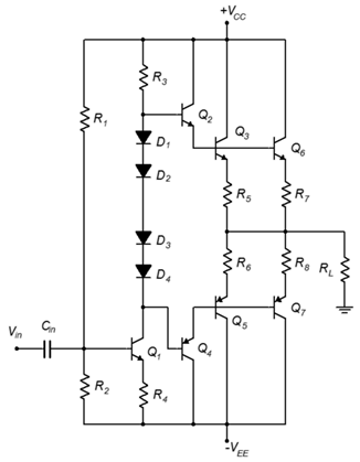
Figure \(\PageIndex{6}\)
9.5.4: Computer Simulation Problems
19. Perform a transient analysis on the circuit of Problem 1 to verify the compliance.
20. Perform a transient analysis on the circuit of Problem 4 to verify the compliance.
21. Perform a DC analysis on the design from Problem 15 to verify the results.
22. Perform a DC analysis on the design from Problem 17 to verify the results.
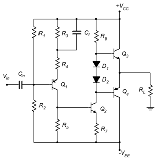
Figure \(\PageIndex{7}\)