
12.2: The DE-MOSFET
- Page ID
- 25327

Like the JFET, the DE-MOSFET is based around the idea of modulating current flow through the drain-source channel by generating a depletion layer from a gate-source voltage. It achieves this through an entirely different process, though. To understand how the device is constructed, a simplified functional drawing of an N-channel DEMOSFET is shown in Figure \(\PageIndex{1}\).
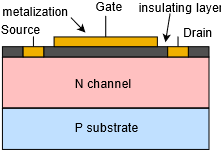
Figure \(\PageIndex{1}\): DE-MOSFET internal structure.
Here we see the N-type channel sitting on a P substrate. Drain and source leads are attached to either end. Above the channel is a very thin insulating layer (silicon dioxide is one possibility). Above this we have a metalization to which the gate terminal is attached. Note that there is no PN junction involved with the gate. To this we shall add external bias sources and limiting resistors, as shown in Figure \(\PageIndex{2}\).
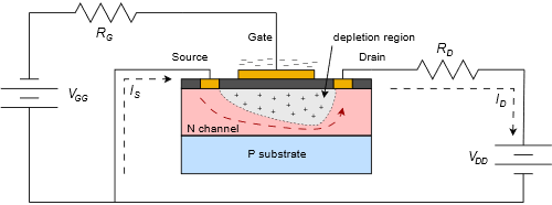
Figure \(\PageIndex{2}\): DE-MOSFET bias with electron flow.
The dashed lines represent electron current flow as in our previous device analyses. A positive supply, \(V_{DD}\), is attached to the drain via a limiting resistor. A second supply, \(V_{GG}\), is attached to the gate. Gate current can be approximated as zero, so \(V_{GS} = V_{GG}\). If \(V_{GS}\) is zero, a certain amount of current will flow through the channel based on the channel's physical parameters and the applied drain-source potential. For relatively low values of \(V_{DS}\), the channel will behave somewhat like a resistance. This is the same ohmic region as seen with the JFET. As \(V_{DS}\) increases, the channel will saturate and begin to behave like a constant current source. If \(V_{DS}\) is brought too high, the drain current increases sharply as the device enters the breakdown region. The general behavior mimics that of a JFET. Note that the current moves laterally, across the device, so this type of construction is referred to as a lateral MOSFET.
If \(V_{GS}\) is set to a modest negative voltage, a depletion region will develop inside the channel. Basically, the gate is acting like one plate of a capacitor, the channel like the other plate, and the insulating layer is the dielectric. Just like a capacitor, the negative charge on the gate “plate” leads to an equivalent positive charge on the channel “plate”. As the channel is made of N-type material, this action creates a region devoid of free charges, hence a depletion region. This depletion region will lead to pinch-off sooner, and thus a lower current in the saturation region. The more negative \(V_{GS}\) is made, the greater the depletion region and the lower the corresponding drain current. Eventually, if \(V_{GS}\) is brought negative enough, the channel will be blocked and no drain current will flow. This voltage is referred to as \(V_{GS(off)}\) (again). The current produced when \(V_{GS} = 0\) V is likewise referred to as \(I_{DSS}\). This mode of operation is referred to as depletion mode because of the depletion region that is created.
What makes the DE-MOSFET distinct from the JFET is what happens when \(V_{GS} > 0\) volts. In a JFET, this would forward bias the junction and control would be lost. Here, however, a positive \(V_{GS}\) simply reverses the polarities associated with the gate and channel “plates”. Thus, a positive \(V_{GS}\) enhances channel conductivity and drain current increases as \(V_{GS}\) is brought more positive. This mode of operation is called enhancement mode. This also means that \(I_{DSS}\) is no longer the maximum drain current of which the device is capable. A characteristic curve is shown in Figure \(\PageIndex{3}\), below.
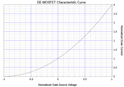
Figure \(\PageIndex{3}\): Characteristic curve for DEMOSFET (note: this uses \(-V_{GS}/V_{GS(off)}\) for the normalized voltage so that the quadrants do not appear reversed compared to a typical device curve).
This curve is essentially the same curve as presented for the JFET with the exception that it extends into the first quadrant. This makes the DE-MOSFET a unique device in that it can operate in two different quadrants.
The device equation for operation when \(V_{DS} > V_P\) is also the same, but with an extended range for \(V_{GS}\):
\[I_D = I_{DSS} \left( 1 − \frac{V_{GS}}{V_{GS (off )}}\right)^2 \label{12.1} \]
Where
\(V_{GS}\) is the gate-source voltage (\(V_{GS(off)} \leq V_{GS} \leq V_{GS(max)})\),
\(I_D\) is the drain current,
\(I_{DSS}\) is the maximum current,
\(V_{GS(off)}\) is the turn-off voltage.
\(V_{GS(max)}\) may be found on a data sheet. Above this voltage the insulating layer will be damaged and the device will cease to function properly. A typical value for this might be in the range of 20 to 30 volts. The trick is that given the very small gate current, even a simple electrostatic discharge can damage the device. It is very easy to develop hundreds of volts static on the human body. In fact, it is generally not noticeable until the potential reaches a few thousand volts (as in body hair standing up). The consequence of this is that simply picking up the device could destroy it.1
There are a couple different ways of dealing with this issue. The first way is to add back-to-back Zener diodes across the device during its manufacture. The problem with this is that the diode leakage current will be greater than the gate current and this degrades performance. The other technique is to prevent the charge from getting to the device in the first place. For example, the MOSFET can be shipped in conductive plastic (not to be confused with ordinary plastic or polystyrene foam). Some devices are shipped with a metal shorting that encompasses all of the leads. Also, during manufacture or prototyping, environmental controls are established to minimize the creation of static charges, optimal humidity being important as one example. Workers who handle devices may work on special conductive mats or wear wrist straps that are attached to ground. These items are only mildly conductive, that is, of high resistance, as it would not be safe to electrically ground a human working in an electrical lab. The devices are conductive enough to bleed off static charge but not so conductive as to present a shock hazard. Once installed on the circuit board, normal ESD precautions apply. As the device's characteristic equation has not changed, many of the items derived for the JFET still apply to the DE-MOSFET. This includes the transconductance equation plot found in Chapter 10.
As the transconductance equation is unchanged with the exception of an extended range for \(V_{GS}\), the definition for \(g_{m0}\) is also unchanged.
\[g_{m0} =− \frac{2 I_{DSS}}{V_{GS(off )}} \label{12.2} \]
\[g_m = g_{m0} \left( 1 − \frac{V_{GS}}{V_{GS (off )}} \right) \label{12.3} \]
It is worth noting that \(g_{m0}\) no longer represents the maximum device transconductance because \(I_{DSS}\) no longer represents the maximum drain current as seen in Figure \(\PageIndex{3}\). To illustrate it another way,
\[g_m = g_{m0} \sqrt{\frac{I_D}{I_{DSS}}} \label{12.4} \]
It is very important to watch the sign of \(V_{GS}\) in Equation \ref{12.3}. In enhancement mode, a positive \(V_{GS}\) will lead to a \(g_m\) greater than \(g_{m0}\) due to the double negative.
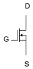
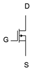
Figure \(\PageIndex{4}\): DE-MOSFET schematic symbols. N-channel (left) and P-channel (right).
The schematic symbols for the DE-MOSFET are shown in Figure \(\PageIndex{4}\). As is the norm, the arrow points in the direction of N material, with the central vertical bar representing the channel. The arrow is attached to the substrate. In some devices this is brought out of the packaging as a fourth lead although in many it is simply tied back to the source terminal as shown here. Finally, note how the gate terminal is not drawn connected to the body of the device, emphasizing its isolated nature.
References
1Which brings to mind the old question of what to store a universal solvent in.