
14.4: Output Configurations
- Page ID
- 25343

If we apply the switching concept to a dual supply, push-pull topology, we arrive at the generic circuit of Figure \(\PageIndex{1}\).
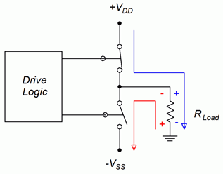
Figure \(\PageIndex{1}\): Generic push-pull switching.
The two output devices are alternately switched on and off. When the upper device is on, the lower device is off, and current flows from the positive supply to the load (blue path). Alternately, when the lower device is on, the upper device is off, and current flows through the load via \(V_{SS}\) (red path). We could use either BJTs or EMOSFETs for these devices.
Two obvious variations exist of the generic output circuit. The first version, shown in Figure \(\PageIndex{2}\), appears to be a direct take-off of a class B output. It is shown with EMOSFETs but could be made with BJTs. Biasing details are not shown, instead a generic “driver” circuit block will prove sufficient for our discussion.
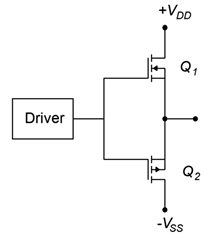
Figure \(\PageIndex{2}\): Basic push-pull switching.
In this circuit, the driver produces a bipolar pulse train that swings from negative to positive rather than from ground to positive. A positive level from the driver will turn on the upper N-channel device, allowing current flow to the load. In contrast, a negative level will turn on the lower P-channel device, allowing load current flow via \(V_{SS}\).1 It is worth noting that the gate drive signal must swing higher and lower than the two power supplies. This is because when a device is on, \(V_{DS}\) will be nearly zero, meaning that the source will be at the power rail. As \(V_{GS}\) must be greater than \(V_{GS(th)}\), this means that \(V_G\) must be greater than the power supply.
An alternate connection scheme is shown in Figure \(\PageIndex{3}\). Here, the N- and P-channel devices have switched positions.
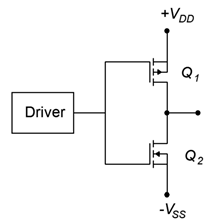
Figure \(\PageIndex{3}\): Alternate push-pull switching.
The logic here is reversed: the negative pulse turns on the upper device and the positive pulse turns on the lower device. The gate swing is lessened a little compared to the earlier circuit but it suffers from a flaw common to both configurations, namely, asymmetry between the N- and P-channel device characteristics. This includes variations between internal device capacitances and \(r_{DS(on)}\) values. For the best possible matching, and thus the lowest distortion and highest performance, it would be better to configure the output using identical devices. This is shown in Figure \(\PageIndex{4}\).
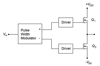
Figure \(\PageIndex{4}\): Output switching using identical devices.
This configuration complicates the drive signal in that we can no longer drive both gates with the same signal; instead, unique signals must be presented to each gate terminal. This circuit is known as a half bridge. Our final step will be to drive both ends of the load in differential fashion using a full bridge, or H bridge as it is sometimes known. This is shown in Figure \(\PageIndex{5}\).
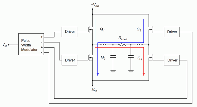
Figure \(\PageIndex{5}\): Full bridge output.
The output devices are controlled as diagonal pairs. When \(Q_1\) is on, \(Q_4\) is on, creating a path for load current from left to right (red trace). In contrast, when \(Q_2\) is on, \(Q_3\) will also be on, thus creating a load current path from right to left (blue trace). This effectively doubles the current amplitude which quadruples the load power (because power varies as the square of current). This is the same technique discussed in Chapter 9 with class B amplifiers. A dual \(L_C\) filter is included in this diagram to remove unwanted frequency components.
Example \(\PageIndex{1}\)
A pair of E-MOSFETs are configured to drive an 8 \( \Omega \) load as in Figure \(\PageIndex{4}\). Assuming that \(\pm\)50 volt sources are used and that each device has an \(r_{DS(on)}\) of 0.03 \( \Omega \), determine the peak load current and \(V_{DS}\) for the MOSFETs.
At any given time, one MOSFET will be on, creating a path between one supply, itself, the load and ground. The total resistance to limit the current will be the load plus \(r_{DS(on)}\).
\[i_{load} = \frac{V_{DD}}{r_{load} + r_{DS (on)}} \nonumber \]
\[i_{load} = \frac{50 V}{8 \Omega +0.03 \Omega} \nonumber \]
\[i_{load} = 6.227A \nonumber \]
The device voltage is found via Ohms law as load and drain current are identical.
\[v_{DS} = i_{load} r_{DS (on)} \nonumber \]
\[v_{DS} = 6.227A \times 0.03 \Omega \nonumber \]
\[v_{DS} = 0.19V \nonumber \]
Practical Concerns
There are a few details left that should not be overlooked. Two of them are related to the edge transition areas, another concerns the complexity of the drive circuits, and the final issue deals with the power supplies themselves
The first item of concern is precisely what happens during the transition. All of the output forms we have examined utilize two active devices configured in series between two power sources. There is nothing in that path to limit current. If both devices were to be simultaneously triggered to the on-state, a huge and possibly damaging current would flow. While it would be foolish to turn both devices on intentionally, the rise and fall times of the pulses effectively do this. As one device is turning on and the other is turning off, both devices are in a conducting state, even if it's not maximum conduction. Essentially, we have two low impedance devices in series between two sources. This results in a large current pulse known as shoot-through. This situation is depicted in Figure \(\PageIndex{6}\).
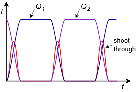
Figure \(\PageIndex{6}\): Shoot-through.
The current pulses for the two devices are shown in blue and violet. The maximal currents are directed to the load, but during the transition, a pulse of current, shown in red, “shoots through” the two devices, from one power supply directly to the other.
The solution to shoot-through is to adjust the turn-on and turn-off pulse timing so as to create a dead time, that is, a time span when neither device is directed to turn on. This is illustrated in Figure \(\PageIndex{7}\).
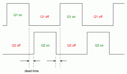
Figure \(\PageIndex{7}\): Dead time.
Dead time is adjusted to correspond with the rise and fall times of the output devices. Basically, a device is not allowed to turn on until the other device is, indeed, fully off. The inclusion of dead time alters the width of the pulse and consequently can introduce waveform distortion. A minimum amount of dead time should be used to avoid this. This is another reason to use very fast output devices as they will require shorter dead times.
The second issue regarding timing is one of device capacitance. Power MOSFETs exhibit relatively high device capacitances. For example, the FDMS86180 examined in Chapter 12 exhibits input and output capacitances of roughly 4.4 nF and 2.7 nF, respectively. Although the extremely high gate input resistance might seem to indicate that very little drive current is needed to turn these devices on, the capacitance tells a different story.
The rate of change of voltage across a capacitor is a function of the capacitance and the current driving it:
\[\frac{dv_C}{dt} = \frac{i_C}{C} \nonumber \]
The larger the current, or the smaller the capacitor, the greater the rate of change of voltage. This can place a serious limit on how quickly a device may be controlled. For example, suppose the drive circuit can pump out up to 10 mA. At first glance that may seem like an enormous amount of current to drive a MOSFET. Now, consider what happens if the input capacitance is 2 nF:
\[\frac{dv_C}{dt} = \frac{i_C}{C} \nonumber \]
\[\frac{dv_C}{dt} = \frac{10mA}{2 nF} \nonumber \]
\[\frac{dv_C}{dt} = 5 E 6 V/s \nonumber \]
While a 5 million volt-per-second slope might sound fast, it's only 5 volts per microsecond. Compared to the requirements of, say, a 200 kHz to 300 kHz switching frequency, that is horribly slow.
Computer Simulation
To see the effect of input capacitance, a two-stage amplifier is captured in a simulator, as shown in Figure \(\PageIndex{8}\). The circuit consists of a relatively standard small signal amplifier feeding a medium power E-MOSFET, the IRF7201. A 10 kHz square wave is used to drive the circuit. The input capacitance of the MOSFET is 550 pF, certainly larger than a small signal FET but not an extremely large value. A single capacitor is placed across the gate that will be used to simulate a much larger device and the associated increased input capacitance.
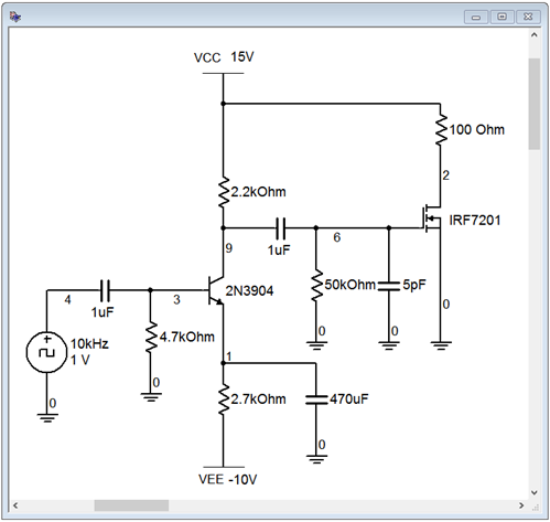
Figure \(\PageIndex{8}\): Circuit for input capacitance testing.
The initial transient analysis is run using a 5 pF gate capacitance which has no appreciable effect on the outcome. The result of the simulation is shown in Figure \(\PageIndex{9}\).
The red trace is the gate voltage at node 6 while the blue trace is the final output at node 2. The gate drive signal is suffering somewhat at the upper portion and the rise and fall times are evident. The output signal is swinging from the power supply of +15 volts down to ground, as expected. The rise time is somewhat quicker than the fall time but, in general, the output presents a decent square pulse at close to 50% duty cycle. The simulation is repeated but this time the gate capacitance is increased from 5 pF to 5 nF, a value more typical of a large power FET. The result is shown in Figure \(\PageIndex{10}\). The red gate drive signal has taken a serious hit and is no longer square in shape. The output pulse in blue still runs to and from the expected voltage levels, but the rising and falling edges are noticeably slowed. Also, the positive pulse width has been stretched due to the slowing of the gate signal which retards the turn on of the MOSFET. The result is a duty cycle that is greater than 50%.
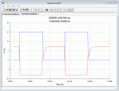
Figure \(\PageIndex{9}\): Waveforms for normal circuit.
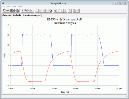
Figure \(\PageIndex{10}\): Waveforms for circuit with increased gate capacitance.
The bottom line is that, in order maximize speed, care must be taken to minimize capacitance, decrease the output impedance of the driver circuit and increase the drive current. Fortunately, this issue has been largely solved by IC manufacturers who offer FET driver integrated circuits designed specifically for these applications.
The final item of practical concern is the power supply itself, or more precisely, the quality of the supply voltage. Remember, the output device is being used as a switch. When the device is on, the power supply is directly connected to the output (with the exception of the small voltage drop across the output device). This means that any noise or ripple on the power supply will make its way to the output filter. Whatever noise components fall within the desired input signal range will not be filtered out, and thus are delivered to the load. In short, the output devices will “leak” the power supply noise into the output, so care must be taken to have as clean of a power supply voltage as possible.
References
1Yes, it is labeled \(V_{SS}\) in spite of the fact that it's connected to the drain of the P-channel device. It's a matter of consistency with other circuits. “A rose by any other name” and all that...