
22.11: Metal Oxide Semiconductor Field Effect Transistor (MOSFET)
- Page ID
- 46344
")
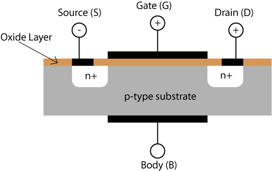
The metal oxide semiconductor field effect transistor (MOSFET) is one of the cornerstones of modern semiconductor technology. The general structure is a lightly doped p-type substrate, into which two regions, the source and the drain, both of heavily doped n-type semiconductor have been embedded.The symbol n+ is used to denote this heavy doping.
The source and the drain are about 1 μm apart. Metallized contacts are made to both source and drain, generally using aluminium. The rest of the substrate surface is covered with a thin oxide film, typically about 0.05 μm thick. The gate electrode is laid on top of the insulating oxide layer, and the body electrode in the above diagram provides a counter electrode to the Gate. The thin oxide film contains silicon dioxide (SiO2), but it may well also contain silicon nitride (Si3N4) and silicon oxynitride (Si2N2O).
The p-type doped substrate is only very lightly doped, and so it has a very high electrical resistance, and current cannot pass between the source and drain if there is zero voltage on the gate. Application of a positive potential to the gate electrode creates a strong electric field across the p-type material even for relatively small voltages, as the device thickness is very small and the field strength is given by the potential difference divided by the separation of the gate and body electrodes.
Since the gate electrode is positively charged, it will therefore repel the holes in the p-type region. For high enough electrical fields, the resulting deformation of the energy bands will cause the bands of the p-type region to curve up so much that electrons will begin to populate the conduction band. This is depicted in the animation below which shows a cross section through the region of the p-type material near the gate electrode. Click the button to increase the voltage applied to the gate electrode.