1.7: Resistance and Conductance
- Last updated
- Save as PDF
- Page ID
- 52872
\( \newcommand{\vecs}[1]{\overset { \scriptstyle \rightharpoonup} {\mathbf{#1}} } \)
\( \newcommand{\vecd}[1]{\overset{-\!-\!\rightharpoonup}{\vphantom{a}\smash {#1}}} \)
\( \newcommand{\id}{\mathrm{id}}\) \( \newcommand{\Span}{\mathrm{span}}\)
( \newcommand{\kernel}{\mathrm{null}\,}\) \( \newcommand{\range}{\mathrm{range}\,}\)
\( \newcommand{\RealPart}{\mathrm{Re}}\) \( \newcommand{\ImaginaryPart}{\mathrm{Im}}\)
\( \newcommand{\Argument}{\mathrm{Arg}}\) \( \newcommand{\norm}[1]{\| #1 \|}\)
\( \newcommand{\inner}[2]{\langle #1, #2 \rangle}\)
\( \newcommand{\Span}{\mathrm{span}}\)
\( \newcommand{\id}{\mathrm{id}}\)
\( \newcommand{\Span}{\mathrm{span}}\)
\( \newcommand{\kernel}{\mathrm{null}\,}\)
\( \newcommand{\range}{\mathrm{range}\,}\)
\( \newcommand{\RealPart}{\mathrm{Re}}\)
\( \newcommand{\ImaginaryPart}{\mathrm{Im}}\)
\( \newcommand{\Argument}{\mathrm{Arg}}\)
\( \newcommand{\norm}[1]{\| #1 \|}\)
\( \newcommand{\inner}[2]{\langle #1, #2 \rangle}\)
\( \newcommand{\Span}{\mathrm{span}}\) \( \newcommand{\AA}{\unicode[.8,0]{x212B}}\)
\( \newcommand{\vectorA}[1]{\vec{#1}} % arrow\)
\( \newcommand{\vectorAt}[1]{\vec{\text{#1}}} % arrow\)
\( \newcommand{\vectorB}[1]{\overset { \scriptstyle \rightharpoonup} {\mathbf{#1}} } \)
\( \newcommand{\vectorC}[1]{\textbf{#1}} \)
\( \newcommand{\vectorD}[1]{\overrightarrow{#1}} \)
\( \newcommand{\vectorDt}[1]{\overrightarrow{\text{#1}}} \)
\( \newcommand{\vectE}[1]{\overset{-\!-\!\rightharpoonup}{\vphantom{a}\smash{\mathbf {#1}}}} \)
\( \newcommand{\vecs}[1]{\overset { \scriptstyle \rightharpoonup} {\mathbf{#1}} } \)
\( \newcommand{\vecd}[1]{\overset{-\!-\!\rightharpoonup}{\vphantom{a}\smash {#1}}} \)
\(\newcommand{\avec}{\mathbf a}\) \(\newcommand{\bvec}{\mathbf b}\) \(\newcommand{\cvec}{\mathbf c}\) \(\newcommand{\dvec}{\mathbf d}\) \(\newcommand{\dtil}{\widetilde{\mathbf d}}\) \(\newcommand{\evec}{\mathbf e}\) \(\newcommand{\fvec}{\mathbf f}\) \(\newcommand{\nvec}{\mathbf n}\) \(\newcommand{\pvec}{\mathbf p}\) \(\newcommand{\qvec}{\mathbf q}\) \(\newcommand{\svec}{\mathbf s}\) \(\newcommand{\tvec}{\mathbf t}\) \(\newcommand{\uvec}{\mathbf u}\) \(\newcommand{\vvec}{\mathbf v}\) \(\newcommand{\wvec}{\mathbf w}\) \(\newcommand{\xvec}{\mathbf x}\) \(\newcommand{\yvec}{\mathbf y}\) \(\newcommand{\zvec}{\mathbf z}\) \(\newcommand{\rvec}{\mathbf r}\) \(\newcommand{\mvec}{\mathbf m}\) \(\newcommand{\zerovec}{\mathbf 0}\) \(\newcommand{\onevec}{\mathbf 1}\) \(\newcommand{\real}{\mathbb R}\) \(\newcommand{\twovec}[2]{\left[\begin{array}{r}#1 \\ #2 \end{array}\right]}\) \(\newcommand{\ctwovec}[2]{\left[\begin{array}{c}#1 \\ #2 \end{array}\right]}\) \(\newcommand{\threevec}[3]{\left[\begin{array}{r}#1 \\ #2 \\ #3 \end{array}\right]}\) \(\newcommand{\cthreevec}[3]{\left[\begin{array}{c}#1 \\ #2 \\ #3 \end{array}\right]}\) \(\newcommand{\fourvec}[4]{\left[\begin{array}{r}#1 \\ #2 \\ #3 \\ #4 \end{array}\right]}\) \(\newcommand{\cfourvec}[4]{\left[\begin{array}{c}#1 \\ #2 \\ #3 \\ #4 \end{array}\right]}\) \(\newcommand{\fivevec}[5]{\left[\begin{array}{r}#1 \\ #2 \\ #3 \\ #4 \\ #5 \\ \end{array}\right]}\) \(\newcommand{\cfivevec}[5]{\left[\begin{array}{c}#1 \\ #2 \\ #3 \\ #4 \\ #5 \\ \end{array}\right]}\) \(\newcommand{\mattwo}[4]{\left[\begin{array}{rr}#1 \amp #2 \\ #3 \amp #4 \\ \end{array}\right]}\) \(\newcommand{\laspan}[1]{\text{Span}\{#1\}}\) \(\newcommand{\bcal}{\cal B}\) \(\newcommand{\ccal}{\cal C}\) \(\newcommand{\scal}{\cal S}\) \(\newcommand{\wcal}{\cal W}\) \(\newcommand{\ecal}{\cal E}\) \(\newcommand{\coords}[2]{\left\{#1\right\}_{#2}}\) \(\newcommand{\gray}[1]{\color{gray}{#1}}\) \(\newcommand{\lgray}[1]{\color{lightgray}{#1}}\) \(\newcommand{\rank}{\operatorname{rank}}\) \(\newcommand{\row}{\text{Row}}\) \(\newcommand{\col}{\text{Col}}\) \(\renewcommand{\row}{\text{Row}}\) \(\newcommand{\nul}{\text{Nul}}\) \(\newcommand{\var}{\text{Var}}\) \(\newcommand{\corr}{\text{corr}}\) \(\newcommand{\len}[1]{\left|#1\right|}\) \(\newcommand{\bbar}{\overline{\bvec}}\) \(\newcommand{\bhat}{\widehat{\bvec}}\) \(\newcommand{\bperp}{\bvec^\perp}\) \(\newcommand{\xhat}{\widehat{\xvec}}\) \(\newcommand{\vhat}{\widehat{\vvec}}\) \(\newcommand{\uhat}{\widehat{\uvec}}\) \(\newcommand{\what}{\widehat{\wvec}}\) \(\newcommand{\Sighat}{\widehat{\Sigma}}\) \(\newcommand{\lt}{<}\) \(\newcommand{\gt}{>}\) \(\newcommand{\amp}{&}\) \(\definecolor{fillinmathshade}{gray}{0.9}\)We have seen that both current and voltage deal with the movement of charge. Consequently, in any electrical system, voltage and current are interrelated. Let us consider the most simple case. This would involve a single voltage source, such as a battery, driving a single, homogeneous item such as a length of wire or a block of a given material. The physical characteristics of this item will dictate how much current will flow. In general terms,
\[Effect = \frac{Cause}{Oppostion} \nonumber \]
In this case the cause is the voltage source and the effect is the resulting current. The opposition is the characteristic of the item in question, in other words, its ability to restrict current flow. We call this characteristic resistance. In other words, resistance is a measure of how difficult it is to establish a flow of current (i.e., “resistance to current flow”) under a given set of circumstances. It is denoted by the letter \(R\) and has units of ohms, in honor of Georg Ohm, a researcher from the early 1800s. The unit is denoted by the capital Greek letter omega, \( \Omega \).
Sometimes it is more convenient to use the inverse view of this phenomenon, and instead of referring to how difficult it is to establish a current, we would be interested in how easy it is to establish a current. This is called conductance and it is the reciprocal of resistance. Conductance is denoted by the letter \(G\) and has units of siemens, named after Werner von Siemens. The unit is abbreviated as S.
\[R = \frac{1}{G} \\ G = \frac{1}{R} \label{2.10} \]
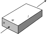
Figure 2.7.1 : Defining resistance.
In this simple scenario, resistance is a function of the material the current is passing through along with its shape. This is illustrated in Figure 2.7.1 where the arrow shows the direction of current flow. An obvious question is “What is this block made of?” It should come as no surprise that the material chosen has a great impact on the current. We have already seen that metals such as copper are good conductors of electricity. Other materials, such as certain plastics and ceramics, are not. These materials are referred to as insulators.
The measure of a material's inherent and general ability to restrict current flow is called resistivity. Resistivity is denoted by the Greek letter \(\rho\) (rho). All other factors being equal, the higher the resistivity, the greater will be the resistance. Further, the greater the length of the material that the current must pass through, the greater the resistance. Finally, as the surface area of the cross section (i.e, the face) grows, the resistance decreases. Expressed as a formula
\[R = \frac{\rho l}{A} \label{2.11} \]
Where
\(R\) is the resistance in ohms,
\(\rho\) is the resistivity,
\(l\) is the length of the material,
\(A\) is area of the face (\(h\) times \(w\)).
Resistivity is often specified in ohm-centimeters with the length and area similarly specified in centimeters and square centimeters, respectively. A table of resistivity values for a variety of materials is shown in Table 2.7.1 . Note that resistivity is not necessarily constant across temperature. Indeed, this change can be exploited as a means of measuring temperature. In other applications, we might need it to be as stable as possible across temperature. This need led to the creation of the alloys Constantan and Manganin in the late 1800s which exhibit very high stability across temperature.
From this table we can see that silver has lower resistivity than copper which in turn is lower than gold. This means that if we made identically sized wires of these three materials, the silver version would have the least resistance and gold the highest. Why then, do audio and video cables often feature gold plating? Certainly, it isn't due to lower resistivity and enhanced conductivity. The reason is that gold is a noble metal, meaning that it does not tarnish. In contrast, the surface of both silver and copper will oxidize, creating a patina (the dark “stain” noticeable on old silver and copper implements). The oxide will create a high resistance layer and reduce the integrity of the connection.
It is important to note that Formula \ref{2.11} does not include a term for the mass of the material. It is only concerned with the shape of the item. This is an important distinction. If we were to alter the mass but keep the ratio of the length versus the area the same, the resulting resistance would be unchanged. In general, the increase in mass by itself does not necessarily alter the resistance but it may have an impact on the power handling capability of the device.
| Material | Resistivity \(\rho (\Omega \cdot \)cm) at 20 \(^{\circ}\)C | Temperature coefficient (K\(^{−1}\)) |
| Silver | 1.59\(\times 10^{−6}\) | 0.0038 |
| Copper | 1.68\(\times 10^{−6}\) | 0.00404 |
| Gold | 2.44\(\times 10^{−6}\) | 0.0034 |
| Aluminium | 2.65\(\times 10^{−6}\) | 0.0039 |
| Zinc | 5.90\(\times 10^{−6}\) | 0.0037 |
| Nickel | 6.99\(\times 10^{−6}\) | 0.006 |
| Iron | 9.7\(\times 10^{−6}\) | 0.005 |
| Platinum | 1.06\(\times 10^{−5}\) | 0.00392 |
| Tin | 1.09\(\times 10^{−5}\) | 0.0045 |
| Titanium | 4.20\(\times 10^{−5}\) | 0.0038 |
| Manganin | 4.82\(\times 10^{−5}\) | 0.000002 |
| Constantan | 4.90\(\times 10^{−5}\) | 0.000008 |
| Stainless steel | 6.90\(\times 10^{−5}\) | 0.00094 |
| Nichrome | 1.10\(\times 10^{−4}\) | 0.0004 |
| Carbon (amorphous) | 5\(\times 10^{−4}\) to 8\(\times 10^{−3}\) | −0.0005 |
| Silicon | 6.4\(\times 10^{4}\) | −0.075 |
| Glass | 1\(\times 10^{13}\) to 1\(\times 10^{17}\) | |
| Carbon (diamond) | 1\(\times 10^{14}\) | |
| Hard rubber | 1\(\times 10^{15}\) | |
| Air | \(10^{11}\) to \(10^{17}\) | |
| PET | 1\(\times 10^{23}\) | |
| Teflon | 1\(\times 10^{25}\) to 1\(\times 10^{27}\) |
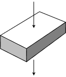
Figure 2.7.2 : Resistance will change due to to altering area and length with mass unchanged.
In contrast, if we take that that original mass and reshape it, or just apply the current to a difference face, such that the effective surface area and length change, then the resulting resistance will also change. This is illustrated in Figure 2.7.2 . Here we have taken the item shown in Figure 2.7.1 and directed the current flow from top to bottom rather than through the side. In this orientation, the surface area is much increased and the length through which the current must travel is greatly reduced. Consequently, the effective resistance in this orientation will be considerably less than that seen in the original.
Example 2.7.1
A certain material has a resistivity of 0.2 ohm-centimeters. Determine the resistance of a piece that is 0.3 cm wide, 0.5 cm high and 4 cm long.
\[A = h \times w \nonumber \]
\[A = 0.5cm \times 0.3cm \nonumber \]
\[A = 0.15 cm^2 \nonumber \]
\[R = \frac{ \rho l}{A} \nonumber \]
\[R = \frac{0.2 \Omega cm \times 4cm}{0.15cm^2} \nonumber \]
\[R = 5.333 \Omega \nonumber \]
For our next example, let's consider a spool of wire. In many cases we treat wire ideally, as if it has no resistance. While this can be a good approximation in many instances, especially with relatively short runs of wire, such is not always the case.
Example 2.7.2
A certain gauge of copper wire has a diameter of 0.6 mm. Determine the resistance if the spool is 200 meters long.
Table 2.7.1 indicates that the resistivity of copper is 1.68E−6 ohm-centimeters. The trick here is that we must keep the units consistent. As there are 100 centimeters to the meter, the length is 200 meters times 100, or 20,000 centimeters (i.e., 20E3). Given that there are 10 millimeters to the centimeter, the diameter must be decreased by a factor of ten, yielding a diameter of 0.06 cm and thus a radius of 0.03 cm.
\[A = \pi r^2 \nonumber \]
\[A = \pi (0.03cm)^2 \nonumber \]
\[A = 2.83E-3cm^2 \nonumber \]
\[R = \frac{ \rho l}{A} \nonumber \]
\[R = \frac{1.68E-6 \Omega cm \times 20E3 cm}{2.83E-3cm^2} \nonumber \]
\[R = 11.9 \Omega \nonumber \]
The amount of resistance seen in Example 2.7.2 would be considered excessive if the item to be connected is something as simple as a loudspeaker, which typically would be around 8 \( \Omega \). And while no one would likely need 200 meters of cable to connect a loudspeaker in their home, that sort of distance would be unremarkable in a large stadium or airport terminal. Don't forget, we'd need wire to and from the loudspeaker, achieving a total separation of 100 meters at most.
Various thicknesses of cables and wires are used for a wide variety of purposes. To make this easier, wire thicknesses have been standardized. The most common standard in North America is the American Wire Gauge, or AWG. This is a nonmetric specification with origins in the mid nineteenth century. The larger the gauge number, the smaller the wire diameter, and the less current it safely can carry. To put the gauge numbers in perspective, typical small home appliances use 16 or 18 gauge wire, basic home wiring uses 12 gauge (with a 20 amp circuit breaker), and hook-up wire used in an electrical circuits or electronics laboratory solderless breadboard is commonly 22 or 24 gauge.
For general purpose wiring, copper is by far the most common metal used because it is highly conductive and relatively inexpensive. Some other metals are used in special cases, for instance, aluminum is used for long distance power transmission lines.
| AWG | Diameter (in) | Diameter (mm) | Resistance/length (\(\Omega\)/km) | Resistance/length (\(\Omega\)/1000ft) |
| 0000 (4/0) | 0.4600 | 11.684 | 0.1608 | 0.04901 |
| 00 (2/0) | 0.3648 | 9.266 | 0.2557 | 0.07793 |
| 0 (1/0) | 0.3249 | 8.251 | 0.3224 | 0.09827 |
| 2 | 0.2576 | 6.544 | 0.5127 | 0.1563 |
| 4 | 0.2043 | 5.189 | 0.8152 | 0.2485 |
| 6 | 0.1620 | 4.115 | 1.296 | 0.3951 |
| 8 | 0.1285 | 3.264 | 2.061 | 0.6282 |
| 10 | 0.1019 | 2.588 | 3.277 | 0.9989 |
| 12 | 0.0808 | 2.053 | 5.211 | 1.588 |
| 14 | 0.0641 | 1.628 | 8.286 | 2.525 |
| 16 | 0.0508 | 1.291 | 13.17 | 4.016 |
| 18 | 0.0403 | 1.024 | 20.95 | 6.385 |
| 20 | 0.0320 | 0.812 | 33.31 | 10.15 |
| 22 | 0.0253 | 0.644 5 | 52.96 | 16.14 |
| 24 | 0.0201 | 0.511 | 84.22 | 25.67 |
| 26 | 0.0159 | 0.405 | 133.9 | 40.81 |
| 32 | 0.00795 | 0.202 | 538.3 | 164.1 |
| 40 | 0.00314 | 0.0799 | 3441 | 1049 |
A table of gauge sizes and associated parameters is shown in Table 2.7.2 . This table assumes copper is being used for the wire. Note that as the diameter of the wire decreases, the amount of resistance for a particular length increases, as expected from Equation \ref{2.11}.
Using this table we can perform a quick crosscheck of Example 2.7.2 . The wire diameter used in that example was 0.6 mm which is just a little smaller than AWG 22 as listed in the table. Further, #22 wire is listed as having a resistance of approximately 53 \( \Omega \) per km. For 200 meters, as used in the example problem, this works out to 10.6 \( \Omega \). As #22 wire is slightly larger in diameter, we expect it to show slightly less resistance than the calculated value of 11.9 \( \Omega \), which it does.
While it may not be immediately apparent, gauge numbers proceed in a logarithmic fashion based on diameter. Stepping up one gauge number (e.g., from #10 to #11) decreases the diameter by a factor of approximately 0.89. As resistance is inversely proportional to the square of the diameter (i.e., the area), the resistance increases by over 25%. Even numbered sizes are particularly common in use and a jump to the next higher even gauge number (e.g., #18 to #20) produces a resistance increase of nearly 60%.
Resistors and the Resistor Color Code
Resistors are devices used to control the currents and voltages in a circuit. They are available in many shapes and sizes, and are normally designed to maintain stable ohmic values in spite of environmental changes such as temperature and humidity. A sample of different resistor styles is shown in Figure 2.7.3 . As a general rule, the larger the resistor, the more power it can handle. At the back of the figure is a large ceramic power resistor using a rectangular aluminum housing. This device is rated for 200 watts of dissipation. Immediately in front and to the right of it are several smaller ceramic power resistors with ratings in the 5 to 20 watt range. Along the left side is a set of carbon composition and carbon film resistors ranging from 1 watt down to one-tenth watt in dissipation. Toward the center is a multi-lead chip resistor that contains several resistors in one package. With few exceptions, all of these items are classified as “through-hole” components, that is, their leads are designed to go through pre-drilled holes in a printed circuit board. These are also the most commonly used components in an electrical lab as the leads fit into solderless breadboards and the components are a convenient size.
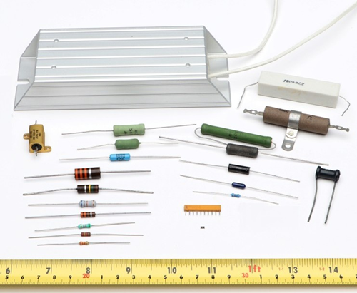
Figure 2.7.3 : A variety of different resistors.
With the increasing desire to shrink components, modern production designs use surface mounting techniques in place of through-hole construction. At the bottom-center is a small dot which is, in fact, a surface mount resistor capable of 1/2 watt of power dissipation. A close-up is shown in Figure 2.7.4 . Obviously, these devices are too small to be practical to use without special equipment.

Figure 2.7.4 : Close up of a surface mount resistor.
Resistors are linear bilateral devices. Being linear, their current-voltage relation can be drawn as a straight line. Bilateral means that the polarity of voltage or direction of current will not matter. In other words, unlike a battery, these devices cannot be inserted into a circuit backwards because either orientation works the same way. If the horizontal axis is voltage and the vertical is current, then the slope of the line yields the conductance. Thus, the steeper the line, the lower its resistance. This is illustrated in Figure 2.7.5 .
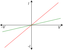
Figure 2.7.5 : Current-voltage plot of two resistors.
Not all electrical components are linear and bilateral. A good example is the semiconductor diode, a commonly used device in electronic systems. The current-voltage plot of a diode is shown in Figure 2.7.6 for comparison. Note that the plot is not a simple straight line, thus it is not linear. Further, the first and third quadrant responses are wildly different, indicating that polarity is of utmost importance. Clearly, it matters which way these kinds of devices are inserted into a circuit.
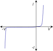
Figure 2.7.6 : Current-voltage plot of a diode: neither linear nor bilateral.
Resistors are available in standardized ohmic values and at standardized power ratings (see Appendix A). Along with their resistance value, resistors also have a specified tolerance. This specifies an allowable range of variation of the stated value. For example, a 220 ohm resistor may have a tolerance of 10%. This means that the actual value of any given specimen from a box of these resistors may be off of the nameplate or nominal value by 10% or 22 ohms. Thus, any particular resistor might be as high as 242 ohms or as low as 198 ohms.
General purpose resistors use a color code to denote their value and tolerance. Typically, this will involve four color stripes: two for the precision/mantissa, one for the power of ten, and the fourth to indicate the tolerance. For higher precision, a five stripe version may be used with the first three denoting the precision/ mantissa. Alternately, high precision resistors may have their nominal value printed directly on them. Refer to Figure 2.7.7 for an example of the basic variety.

Figure 2.7.7 : Example of basic four stripe resistor color code.
The first two bands, here yellow and violet, indicate the precision or leading digits. The third band, here orange, indicates the power of ten or “number of zeroes” to add. The fourth band, silver in this example, indicates the tolerance. Note that the fourth band is spaced away from the others to avoid accidentally reversing the order.
The color code is shown in Figure 2.7.8 . To assist in remembering the sequence, a number of mnemonic aids have been used, the first letter of each word starting with the same letter as the corresponding color. One example is the “Picnic Basket Mnemonic” which is: Black Bears Robbed Our Yummy Goodies Beating Various Gray Wolves. Another possibility is to note that the middle section follows a rainbow with black and white at the extreme ends.
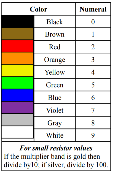
Figure 2.7.8 : Resistor color code.
The tolerance band colors are as follows: For basic parts silver is \(\pm\)10% and gold is \(\pm\)5%. If the fourth band is omitted, this indicates a tolerance of \(\pm\)20%, although it is seldom used in modern designs. For precision parts some colors are reused but follow the color code numerals: Brown is \(\pm\)1% tolerance and red is \(\pm\)2% tolerance. Tighter tolerances are also available. Sometimes an extra band is added that indicates a reliability rating or temperature coefficient. In such cases, it is best to refer to the manufacturer's data sheets for details. We will not pursue these further.
Example 2.7.3
Determine the nominal, maximum and minimum acceptable resistance values for the resistor pictured in Figure 2.7.2 .
The colors are yellow-violet-orange. This translates to 4, 7 and 3. The value is “47 with 3 zeroes”, or 47000 ohms. The silver fourth band indicates 10% tolerance. Thus, the resistor pictured is nominally 47 k\( \Omega \) with \(\pm\)10% variation around the nominal value being acceptable. The tolerance yields \(\pm\)4.7 k\( \Omega \), so the acceptable range is from 42.3 k\( \Omega \) to 51.7 k\( \Omega \).
Example 2.7.4
A precision resistor has a color code of orange-blue-green-brown-brown. Determine its value and acceptable range.
The final band indicates that this is a \(\pm\)1% tolerance component. The first four colors translate to 3, 6, 5 and 1. The value is “365 with 1 zero”, and thus 3650 ohms, or 3.65 k\( \Omega \). The allowable range is 3.65 k\( \Omega \) \(\pm\) 36.5 \( \Omega \).
Example 2.7.5
Determine the nominal value and tolerance of a resistor with the color code green-blue-gold-silver.
The first two colors translate to 5 and 6. Gold in the third band means “multiply by 0.1”. The final band indicates that this is a \(\pm\)10% tolerance component. Therefore, nominal value is 5.6 \( \Omega \). The allowable range is 5.6 \( \Omega \) \(\pm\) 0.56 \( \Omega \).
An example of a resistor data sheet is shown in Figure 2.7.9 . This data sheet is for a series of surface mount chip resistors. The available tolerance grades range from 0.5% to 20%. Also, for each variant there are two temperature coefficients available with the most stable being 100 ppm/\(^{\circ}\)C (ppm is short for “parts per million”, thus 100 ppm is equivalent to 0.01%). Note that these devices are too small to use the resistor color code. Instead, a numeric code is printed directly on them that follows the rules for color bands, meaning that the final digit is the multiplier. Thus “150” is 15 \( \Omega \) (1-5 with no zeroes). The exception is very small values where the letter “R” is used in place of a decimal point. Consequently, “2R4” is 2.4 \( \Omega \).

Figure 2.7.9 : Example resistor data sheet. Courtesy of Stackpole Electronics
A particularly important characteristic of most electronic devices is their power handling capacity. For this series there are several variations with power handling from 0.1 watts to 1.5 watts, and maximum working voltages up to 500 volts. Power handling is also a function of ambient temperature. In general, devices have a maximum internal temperature that they can reach before they are damaged. Control of heat tends to be a major issue in many system designs. If the ambient temperature increases, there is less “headroom” for the device's temperature rise, and thus the device will not be able to dissipate as much power. This is illustrated in the graph of Figure 2.7.10 .
Note how the power dissipation is constant at temperatures at and below 70 \(^{\circ}\)C. This temperature is considered the maximum normal operating temperature for this device and the power dissipation at this temperature is the one quoted in the data sheet. If the device is operated in a warmer environment, the power dissipation is derated by the percentage given in the graph. For example, at 100 \(^{\circ}\)C the dissipation is only about 65% of the nominal rating. Of particular importance, at 155 \(^{\circ}\)C the device can no longer dissipate any power, and therefore this temperature serves as the absolute ceiling. After all, a resistor that cannot dissipate any power is a resistor that cannot have any current through it or voltage across it without burning up. It is essentially non-functional.
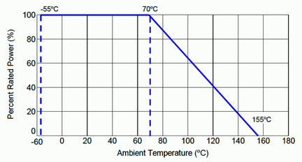
Figure 2.7.10 : Resistor power derating graph. Courtesy of Stackpole Electronics
Of course, just like a skillet on a stove, these devices do not heat up instantly, that is, they exhibit a thermal time constant. They take a certain amount of time to heat (and also to cool). For short periods, devices can handle considerably more power than their long term rating. The graph of Figure 2.7.11 , shows the power dissipation for single pulses. In some cases, these resistors can handle powers of an order of magnitude greater. For example, consider the type RPC0402 (bottom-most line). From the data sheet of Figure 2.7.9 this device is specified as having a long term rating of 0.2 watts. In contrast, the graph of Figure 2.7.11 shows it is capable of withstanding a single pulse of greater than 20 watts for 100 microseconds, just under 10 watts for a millisecond pulse and roughly 2 watts for a one-tenth second pulse.
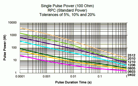
Figure 2.7.11 : Pulse power dissipation. Courtesy of Stackpole Electronics
Other Resistive Devices
Along with standard fixed resistors, there are several other kinds of resistive devices that have been designed to be sensitive to changes in their environment. Thus, they can serve as sensors because as their resistance changes, it impacts the flow of current and the resulting voltage. We will look at examples of this in upcoming work. Some of the environmental inputs include temperature, force and light levels.
Force Sensing Resistor (FSR)
The force sensing resistor consists of two layers of material with a nominal separation distance. It is presented as a flat membrane that is usually round or rectangular, and perhaps with an adhesive backing. An example of an FSR is shown in Figure 2.7.12 . With no force applied, the device shows an extremely high resistance, well into the megohms. As force is applied to the surface, the two layers come into better contact which decreases the net resistance. This is borne out in the graph of Figure 2.7.13 . The graph shows roughly a straight line response between resistance and force when plotted on a log-log scale. At the highest force levels, the resistance may drop to just a few hundred ohms.
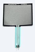
Figure 2.7.12 : A force sensing resistor (FSR).
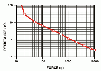
Figure 2.7.13 : FSR response curve. Courtesy of Interlink Electronics
Photoresistor
As their name implies, photoresistors are sensitive to changes in light level. They are also called LDRs, short for Light Dependent Resistor. Different materials may be used in their construction, but the most common is cadmium sulfide, CdS. As a consequence, photoresistors are sometimes generically referred to as “CdS cells”.
A photoresistor is shown in Figure 2.7.14 along with its corresponding resistance graph in Figure 2.7.15 . In total darkness the device exhibits a very high resistance. As light levels increase, the resistance decreases. As with the FSR, we see an reverse relation between the resistance and the environmental factor: as the environmental input increases (force, light level), the resistance does the opposite and decreases. And once again, we see a straight line when plotted with log-log scales. Technically, we refer to this as a negative relation because the slope of the plot line is negative.

Figure 2.7.14 : A photoresitor, or LDR.
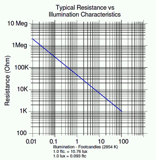
Figure 2.7.15 : Photoresitor response curve. Courtesy of Advanced Photonix
To put the brightness of the light into common terms, 0.01 foot-candles (roughly 0.1 lux) is equivalent to a clear moon-lit evening. At this level, the photoresistor is showing over 1 megohm of resistance. In contrast, 100 foot-candles (roughly 1000 lux) is equivalent to an overcast day (for reference, direct sunlight is perhaps 100 times stronger). At this level, the photoresistor's value has dropped to about 1000 ohms.
A point worth noting is that the light that the photoresistor “sees” is not necessarily the same as what a human sees. The sensitivity of the device at various wavelengths (i.e., colors) may differ starkly from human vision. In fact, differing materials exhibit different sensitivities at various wavelengths. Some of these may be wavelengths that the unaided human eye cannot see at all (infrared or ultraviolet, for example).
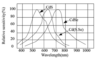
Figure 2.7.16 : Photoresitor sensitivity curves. Courtesy of Token Electronics
An example of sensitivity curves is shown in Figure 2.7.16 . Note the variations between the different materials, CdS being one of the three (left side). The peak sensitivities vary as do the precise shapes. In practice, this means that some of these units will be more or less sensitive to certain colors than other units. The CdS curve indicates peak sensitivity of about 540 nm, which corresponds to green. In comparison, the CdSe (cadmium selenide) cell exhibits a peak of just over 700 nm, which corresponds to red. At some wavelengths, the relative response of one material may be no more than 10% of the response of a different material.
It is important to note that the use of cadmium, such as in CdS cells and the like, is severely restricted by the RoHS directive (see Chapter One).
Thermistor
A thermistor is a device whose resistance is a function of temperature. These devices are available in two basic types. Either PTC, for Positive Temperature Coefficient; or NTC, for Negative Temperature Coefficient. PTC devices show an increase in resistance as temperature increases and NTC devices show a decrease in resistance as temperatures rise. Ideally, these are linear relationships with the plots showing straight lines. The reality is that linearity can only be assumed across fairly narrow ranges of temperature. For wider ranges, there will be noticeable deviation from a straight line as the curve is logarithmic in nature. A basic NTC thermistor is shown in Figure 2.7.17 .

Figure 2.7.17 : NTC thermistor.
Generic thermistor performance graphs are shown in Figure 2.7.17 with the idealized straight line response at top and the more realistic non-linear response below. Thermistors will be specified in terms of their room temperature resistance (usually taken to be 25 \(^{\circ}\)C) along with their sensitivity which is denoted as beta (\(\beta\)). The larger the value of beta, the steeper the curve and the greater the sensitivity. The curves labeled Beta 2 show increased sensitivity, meaning that there will be a greater change in resistance for a certain change in temperature.
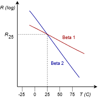
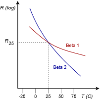
Figure 2.7.18 : NTC thermistor response curves: Ideal (top) and real.
The following equation can be used to determine the resistance of a thermistor at some other temperature of interest with greater accuracy than using a simple linear approximation. All that is needed is a reference temperature and corresponding resistance, the beta value and the new temperature of interest. Using a reference temperature of 25 \(^{\circ}\)C:
\[R_T = R_{25} e^{\beta \left( \frac{1}{T} − \frac{1}{298.15} \right)} \label{2.12} \]
Where
\(R_T\) is the resistance at the new kelvin temperature, \(T\),
\(R_{25}\) is the resistance at 25 \(^{\circ}\)C,
\(T\) is the temperature of interest in kelvin,
\(\beta\) is the device beta.
Note that the constant “298.15” in Equation \ref{2.12} is equivalent to the reference temperature of 25 \(^{\circ}\)C (0 K is −273.15 \(^{\circ}\)C). Consequently, if a different reference point is used, simply insert the new reference temperature in its place and use the corresponding resistance in place of \(R_{25}\).
Varistor
Varistors are used as limiting devices, primarily to suppress unwanted voltage spikes in electronic equipment. The varistor is a unique device in that it has a highly nonlinear current-voltage characteristic. This is shown in Figure 2.7.19 . Remember, when plotted with the voltage on the horizontal axis, the slope of the line represents the conductance. Consequently, the varistor shows a region of near zero conductance or extremely high resistance (the horizontal section), and two sections that are nearly vertical, which indicate extremely high conductance or near zero resistance. This characteristic allows the varistor to act as a limiting device.
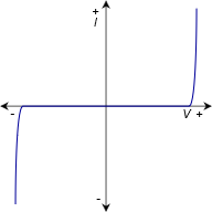
Figure 2.7.19 : Current-voltage characteristic of a varistor
Imagine that a lightning strike effects a local power line. This will create a sudden but short-lived spike in the voltage. A normal 120 volt wall outlet normally produces regular peaks of approximately 170 volts. A lightning strike might add several hundred volts to this. The resulting voltage could be so high that it would damage electronic equipment attached to the outlet. To alleviate this problem, a varistor can be placed across the incoming voltage lines. The vertical break point voltages would be set for a value just over 170 volts, the normal maximum. Under typical circumstances the varistor would see a voltage in its horizontal region and thus behave as a very high resistance. It would drain virtually no current from the outlet, and consequently it would have no impact on the rest of the circuitry. On the other hand, if a large spike hits the line, the varistor will swing into the vertical region, show a much reduced resistance, and act as a shunting path for the spike's current. It will effectively clamp the voltage to some maximum rated value. Of course, the varistor has to absorb the energy presented by that spike, and important parameters of a varistor include the amount of energy that it can absorb (in joules) and its maximum current capacity, along with the maximum clamping voltage.
Strain gauge
The strain gauge is device used to measure mechanical strain on some item. Strain occurs when an item is under compression (its length gets shortened or squished) or when it's under tension (it gets elongated or stretched). Both of these things can happen simultaneously, for example when a bar is experiencing bending or torque (one side is under compression while the other is under tension). Engineering strain is defined as the change in length over the initial length. If an item experiences too much strain, it can become permanently deformed or fail (for example, the landing gear in an aircraft or the suspension components in a car). Simply put, strain gauges are used to measure this effect.
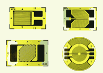
Figure 2.7.20 : Strain guages. Courtesy of Zemic
A strain gauge is made typically of very thin metal foil in a specific pattern. See Figure 2.7.20 for example shapes. Typically, the shape is that of a series of fine lines connected in a back-and-forth pattern, the two ends terminating into larger pads for soldering on connecting leads. In operation, the strain gauge is glued to the material being investigated, for example, a metal bar that is part of a suspension system. As they are glued together, the strain gauge experiences the same deformation as the metal bar. Any deformation will create changes in the length of the strain gauge's foil wires as well as their frontal surface area. For example, under tension, the length increases while the surface area decreases (the surface area must decrease because the foil wire has finite mass). Recalling the basic resistance relation, Equation \ref{2.11}, both of these effects will cause the resistance to rise. The greater the strain under tension, the greater the rise in resistance. The opposite will occur under compression and the resistance will decrease. These changes in resistance are not large but they are sufficient to alter the associated voltage or current which can then be calibrated to determine the applied strain.


