
7.5: The Differential Amplifier
- Page ID
- 52989

Most modern operational amplifiers utilize a differential amplifier front end. In other words, the first stage of the operational amplifier is a differential amplifier. This circuit is commonly referred to as a diff amp or as a long-tailed pair. A diff amp utilizes a minimum of 2 active devices, although 4 or more may be used in more complex designs. Our purpose here is to examine the basics of the diff amp so that we can understand how it relates to the larger operational amplifier. Therefore, we will not be investigating the more esoteric designs. To approach this in an orderly fashion, we will examine the DC analysis first, and then follow with the AC small signal analysis.
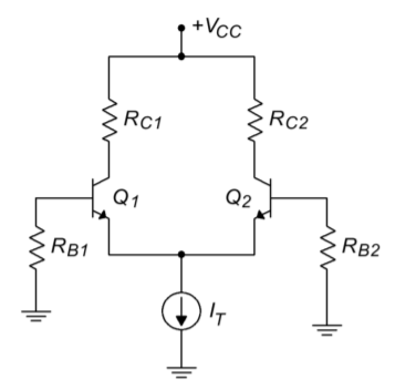
Figure \(\PageIndex{1}\): Simplified diff amp.
1.6.1: DC Analysis
A simplified diff amp is shown in Figure \(\PageIndex{1}\). This circuit utilizes a pair of NPN bipolar transistors, although the circuit could just as easily be built with PNPs or FETs. Note the inherent symmetry of the circuit. If you were to slice the circuit in half vertically, all of the components on the left half would have a corresponding component on the right half. Indeed, for optimal performance, we will see that these component pairs should have identical values. For critical applications, a matched pair of transistors would be used. In this case, the transistor parameters, such as \(\beta\), would be very closely matched for the two devices.
In Figure \(\PageIndex{2}\), the circuit currents are noted, and the generalized current source has been replaced with a resistor/negative power supply combination. This is in essence, an emitter bias technique. Assuming that the base voltages are negligible and that \(V_{BE}\) is equal to 0.7 V, we can see that the emitter of each device is at approximately -0.7 V. Kirchhoff’s Voltage Law indicates that the bulk of the negative supply potential must drop across \(R_T\).
\[ V_{RT} = ∣V_{EE}∣−.7V \nonumber \]
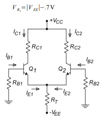
Figure \(\PageIndex{2}\): Diff amp analysis of Figure \(\PageIndex{1}\).
Knowing this, we may find the current through \(R_T\), which is known as the tail current, \(I_T\).
\[ I_T = \frac{∣V_{EE}∣−0.7 V}{R_T} \nonumber \]
If the two halves of the circuit are well matched, the tail current will split equally into two portions, \(I_{E1}\) and \(I_{E2}\). Given identical emitter currents, it follows that the remaining currents and voltages in the two halves must be identical as well. These potentials and currents are found through the application of Kirchhoff’s Voltage and Current Laws just as in any other transistor bias analysis.
Example \(\PageIndex{1}\)
Find the tail current, the two emitter currents, and the two collector to ground voltages in the circuit of Figure \(\PageIndex{3}\). You may assume that the two transistors are very closely matched.
The first step is to find the tail current:
\[ I_T = \frac{∣V_{EE}∣−0.7 V}{R_T} \nonumber \]
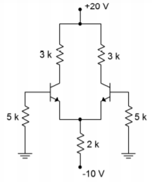
Figure \(\PageIndex{3}\): Diff amp for example \(\PageIndex{1}\).
The tail current is the combination of the two equal emitter currents, so
\[ I_{EI} = I_{E2} = I_{T2} \\ I_{EI} = I_{E2} = \frac{4.65\ mA}{2} \\ I_{EI} = I_{E2} = 2.325\ mA \nonumber \]
If we make the approximation that collector and emitter currents are equal, we may find the collector voltage by calculating the voltage drop across the collector resistor, and subtracting the result from the positive power supply.
\[ V_{c} = V_{cc} - I_c\ R_c \\ V_{c} = 20\ V - 2.325\ mA \times 3k\Omega \\ V_{c} = 20\ V - 6.975\ V \\ V_{c} = 13.025\ V \nonumber \]
Again, because we have identical values for both halves of the circuit, \(V_{C1} = V_{C2}\). If we continue with this and assume a typical \(\beta\) of 100, we find that the two base currents are identical as well.
\[ I_{B} = \frac{I_c}{\beta} \\ I_{B} = \frac{2.325\ mA}{100} \\ I_{B} = 23.25\ \mu A \nonumber \]
Noting that the base currents flow through the 5 k\(\Omega\) base resistors, we may find the base voltages. Note that this is a negative potential because the base current is flowing from ground into the transistor’s base.
\[ V_{B} = -I_b\ R_B \\ V_{B} = −23.25\ \mu A \times 5k\Omega \\ V_{B} = −116.25\ mV \nonumber \]
This result indicates that the actual emitter voltage is closer to -0.8 V than -0.7 V, and thus, the tail current is actually a little less than our approximation of 4.65 mA. This error is probably within the error we can expect by using the 0.7 V junction potential approximation.
1.6.2: Input Offset Current and Voltage
As you have no doubt guessed, it is impossible to make both halves of the circuit identical, and thus, the currents and voltages will never be exactly the same. Even a small resistor tolerance variation will cause an upset. If the base resistors are mismatched, this will cause a direct change in the two base potentials. A variation in collector resistance will cause a mismatch in the collector potentials. A simple \(\beta\) or \(V_{BE}\) mismatch can cause variations in the base currents and base voltages, as well as smaller changes in emitter currents and collector potentials. It is desirable then to quantify the circuit’s performance so that we can see just how well balanced it is. We can judge a diff amp’s DC performance by measuring its input offset current and its input and output offset voltages. In simple terms, the difference between the two base currents is the input offset current. The difference between the two collector voltages is the output offset voltage. The DC potential required at one of the bases to counteract the output offset voltage is called the input offset voltage (this is little more than the output offset voltage divided by the DC gain of the amplifier). In an ideal diff amp all three of these factors are equal to 0. We will take a much closer look at these parameters and how they relate to operational amplifiers in later chapters. For now, it is only important that you understand that these inaccuracies exist, and what can cause them.
1.6.3: AC Analysis
Figure \(\PageIndex{4}\) shows a typical circuit with input and output connections. In order to minimize confusion with the DC circuit, AC equivalent values will be shown in lower case. Small emitter degeneration resistors, \(r_{E1}\) and \(r_{E2}\), have been added to this
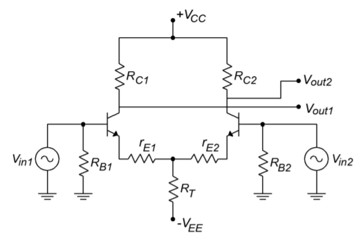
Figure \(\PageIndex{4}\): A typical diff amp with input and output connections.
diff amp. This circuit has two signal inputs and two signal outputs. It is possible to configure a diff amp so that only a single input and/or output is used. This means that there are four variations on the theme:
- Differential (also called dual- or double-ended) input, differential output.
- Differential input, single-ended output.
- Single-ended input, differential output.
- Single-ended input, single-ended output.
These variations are shown in Figure \(\PageIndex{5}\). For use in operational amplifiers, the differential input/single-ended output variation is the most common. We will examine the most general case, the differential input/differential output version.

Figure \(\PageIndex{5}\): The four different diff amp input/output configurations.
Because the diff amp is a linear circuit, we can use the principle of Superposition to independently determine the output contribution from each of the inputs. Utilizing the circuit of Figure \(\PageIndex{4}\), we will first determine the gain Equation from \(V_{in1}\) to either output. To do this, we replace \(V_{in2}\) with a short circuit. The AC equivalent circuit is shown in Figure \(\PageIndex{6}\).
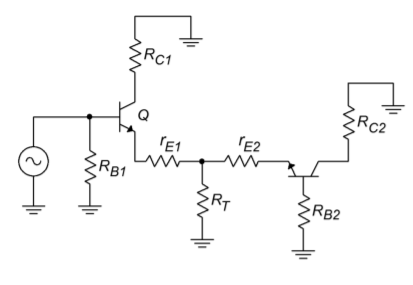
Figure \(\PageIndex{6}\): The circuit of Figure \(\PageIndex{4}\) redrawn for AC analysis.
For the output on collector 1, transistor 1 forms the basis of a common emitter amplifier. The voltage across \(r_{C1}\) is found via Ohm’s Law.
\[ v_{r_{C1}} = −i_{C1}\ r_{C1} \nonumber \]
The negative sign comes from the fact that AC ground is used as our reference. (i.e., for a positive input, current flows from AC ground down through \(r_{C1}\), and into the collector.) To a reasonable approximation, we can say that the collector and emitter currents are identical.
\[ v_{r_{cl}} = −i_{EI}\ r_{C1} \nonumber \]
We must now determine the AC emitter current in relation to \(V_{in1}\). In order to better visualize the process, the circuit of Figure \(\PageIndex{6}\) is altered to include simplified transistor models, as shown in Figure \(\PageIndex{7}\).
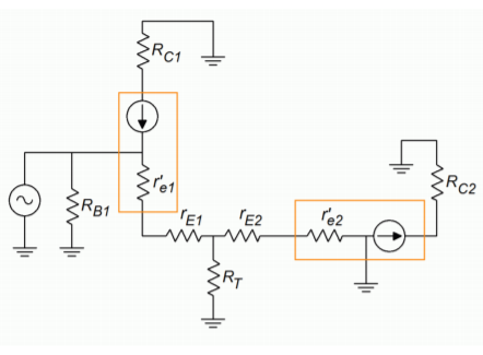
Figure \(\PageIndex{7}\): AC analysis.
\(r^{'}_e\) is the dynamic resistance of the base emitter junctions and is inversely proportional to the DC emitter current. You may recall the following Equation from your prior course work:
\[ r^{'}_e = \frac{26\ mV}{I_E} \nonumber \]
Where
\(r^{'}_e\) is the dynamic base-emitter junction resistance,
\(I_E\) is the DC emitter current.
For typical circuits, the values of \(r^{'}_e\) and \(r_E\) are much smaller than the tail current biasing resistor, \(R_T\). Because of its large size, we can ignore the parallel effect of \(R_T\). By definition, the AC emitter current must equal the AC emitter potential divided by the AC resistance in the emitter section. If you trace the signal flow from the base of transistor 1 to ground, you find that it passes through \(r^{'}_{e1}\),\(r_{E1}\), \(r^{'}_{e2}\) and \(r_{E2}\). You will also notice that the magnitude of \(i_{E1}\) is the same as \(i_{E2}\), although they are out of phase.
\[ i_E = \frac{v_{in1}}{ r^{'}_{e1}+r_{E1}+r^{'}_{e2}+r_{E2}} \nonumber \]
Because the circuit values should be symmetrical for best performance, this Equation may be simplified to
\[ i_E = \frac{v_{in}}{ 2(r^{'}_{e}+r_{E})} \nonumber \]
If we now solve for voltage gain,
\[ A_v = -\frac{v_{out}}{v_{in}} \nonumber \]
\[ A_v = \frac{-i_E\ r_c}{v_{in}} \nonumber \]
\[ A_v = \frac{\frac{v_{in}}{2(r^{'}_{e}+r_{E})} r_c}{v_{in}} \nonumber \]
\[ A_v = \frac{-r_c}{2(r^{'}_{e}+r_{E})} \nonumber \]
Where
\(A_v\) is the voltage gain,
\(r_C\) is the AC equivalent collector resistance,
\(r_E\) is the AC equivalent emitter resistance,
\(r^{'}_{e}\) is the dynamic base-emitter junction resistance.
The final negative sign indicates that the collector voltage at transistor number 1 is 180 degrees out of phase with the input signal. Earlier, we noted that \(i_{E2}\) is the same magnitude as \(i_{E1}\), the only difference being that it is out of phase. Because of this, the magnitude of the collector voltage at transistor number 2 will be the same as that on the first transistor. Because the second current is out of phase with the first, it follows that the second collector voltage must be out of phase with the first. This means that the voltage at the second collector is in phase with the first input signal. Its gain Equation is
\[ A_v = \frac{r_c}{2(r^{'}_{e}+r_{E})} \nonumber \]
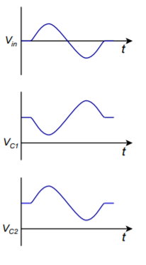
Figure \(\PageIndex{8}\): Waveforms for a single input.
The various waveforms are depicted in Figure \(\PageIndex{8}\). The preceding Equation is often referred to as the single-ended input/single-ended output gain Equation because it describes the single change from one input to one output. The output signal will be in phase if we are examining the opposite transistor, and out of phase if we are looking at the input transistor. Because the circuit is symmetrical, we will get similar results when we examine the second input. The voltage between the two collectors is 180 degrees apart. If we were to use a differential output, that is, derive the output from collector to collector rather than from one collector to ground, we would see an effective doubling of the output signal. If the reason for this is not clear to you, consider the following. Assume that each collector has a 1 V peak sine wave riding on it. When collector 1 is at +1 V, collector 2 is at -1 V, making +2 V total. Likewise, when collector 1 is at its negative peak, collector 2 is at its positive peak, producing a total of -2 V. The single ended input/differential output gain therefore is
\[ A_v = \frac{r_c}{r^{'}_{e}+r_{E}} \nonumber \]
Example \(\PageIndex{2}\)
Using the circuit of Figure \(\PageIndex{4}\), determine the single-ended input/differential output and single-ended input/single-ended output voltage gains. Use the following component values: \(V_{CC} = 15V\), \(V_{EE} = -8V\), \(R_T = 10k\Omega\), \(R_C = 8k\Omega\), \(r_E = 30\Omega\). In order to find \(r^{'}_e\) we must find the DC current.
\[ I_{T} = \frac{∣V_{EE}∣−0.7 V}{R_T} \\ I_{T} = \frac{7.3\ V}{10\ k\Omega} \\ I_{T} = 730\ \mu A \nonumber \]
\[ I_{E} = \frac{I_T}{2} \\ I_{E} = \frac{730\ \mu A}{2} \\ I_{E} = 365\ \mu A \nonumber \]
\[ r^{'}_{e} = \frac{26\ mV}{I_E} \\ r^{'}_{e} = \frac{26\ mV}{365\ \mu A} \\ r^{'}_{e} = 71.2\ \Omega \nonumber \]
For the single ended output gain,
\[ A_v = \frac{r_c}{2(r^{'}_{e}+r_{E})} \nonumber \]
\[ A_v = \frac{8\ k\Omega}{2(71.2\ \Omega+30\ \Omega)} \nonumber \]
\[ A_v = \frac{8\ k\Omega}{202.4\ \Omega} \nonumber \]
\[ A_v = 39.5 \nonumber \]
The differential output gain is twice this value, or 79.
Because it is possible to drive a diff amp with two distinct inputs, a wide variety of outputs may be obtained. It is useful to investigate two specific cases:
- Two identical inputs in both phase and magnitude.
- Two inputs with identical magnitude, but 180 degrees out of phase.
Let’s consider the collector potentials for the first case. Assume that a diff amp has a single-ended input/single-ended output gain of 100 and a 10 mV signal is applied to both bases. Using Superposition, we find that the outputs due to each input are 100 times 10 mV, or 1 V in magnitude. For the first input, the voltages are sketched in Figure \(\PageIndex{9a}\) (following page). For the second input, the voltages are sketched in Figure \(\PageIndex{9b}\). Note that each collector sees both a sine wave and an inverted sine wave, both of equal amplitude. When these two signals are added, the result is zero, as seen in Figure \(\PageIndex{9c}\). In Equation form,
\[ v_{C1} = v_{in1} (−A_v )+v_{in2}\ A_v \nonumber \]
\[ v_{C1} = A_v(v_{in2}−v_{in1}) \nonumber \]
Because \(v_{in1}\) and \(v_{in2}\) are identical, the output is ideally zero given a perfectly matched and biased diff amp. The exact same effect is seen on the opposite collector. This last Equation is very important. It says that the output voltage is equal to the gain times the difference between the two inputs. This is how the differential amplifier got its name. In this case, the two inputs are identical, and thus their difference is zero. On the other hand, if we were to invert one of the input signals(case 2), we find a completely different result.
\[ v_{in1} = -v_{in2} \\ v_{C1} = A_v(v_{in2}-v_{in1}) \\ v_{C1} = A_v(v_{in2}-(-v_{in2})) \\ v_{C1} = 2\ A_v\ v_{in2} \nonumber \]
Thus, if one input is inverted, the net result is a doubling of gain. This effect is shown graphically in Figures \(\PageIndex{9d}\) through \(\PageIndex{9f}\). In short, a differential amplifier suppresses in phase signals while simultaneously boosting out of phase signals. This can be a very useful attribute, particularly in the area of noise reduction.
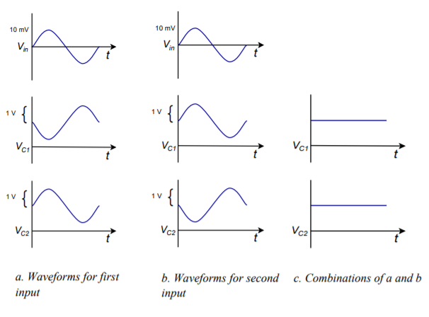
Figure \(\PageIndex{9}\): Input-output waveforms for common mode.
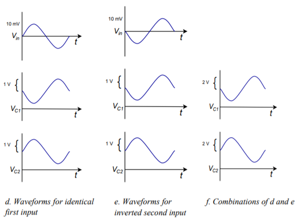
Figure \(\PageIndex{9}\): (continued) Input-output waveforms for common mode.
1.6.4: Common Mode Rejection
By convention, in phase signals are known as common-mode signals. An ideal differential amplifier will perfectly suppress these common-mode signals, and thus, its common-mode gain is said to be zero. In the real world, a diff amp will never exhibit perfect common-mode rejection. The common-mode gain may be made very small, but it is never zero. For a common-mode gain of zero, the two halves of the circuit have to be perfectly matched, and all circuit elements must be ideal. This is impossible to achieve as errors may arise from several sources. The most obvious error sources are resistor tolerance variations and transistor parameter spreads. The basic design of the circuit will also affect the common-mode gain. With some circuit rearrangements, it is possible to determine a common-mode gain for the circuits we have been using. The circuit of Figure \(\PageIndex{4}\) has been redrawn in Figure \(\PageIndex{10}\) in order to emphasize its parallel symmetry.
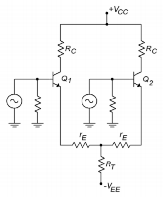
Figure \(\PageIndex{10}\): The circuit of Figure \(\PageIndex{4}\) redrawn for common mode rejection ratio (CMRR) analysis.
Because the DC potentials are identical in both halves, and identical signals drive both inputs, we can combine resistors in parallel in order to arrive at the circuit of Figure \(\PageIndex{11}\).
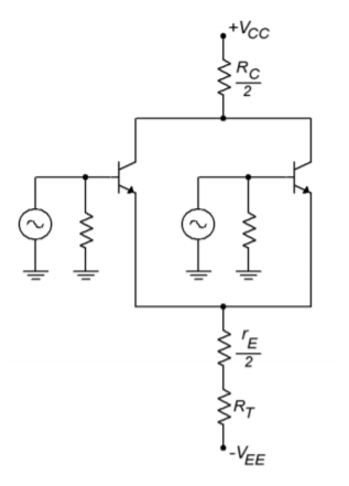
Figure \(\PageIndex{11}\): Common mode gain analysis.
Although it is not shown explicitly on the diagram, the internal dynamic resistances \((r^{'}_e)\) may also be combined (\(r^{'}_{e}/2\)). This circuit has been effectively reduced to a simple common emitter stage. Based on our earlier work, the gain for this circuit is
\[ A_{v(cm)} = \frac{\frac{r_C}{2}}{R_T + \frac{r^{'}_e}{2} + \frac{r_E}{2}} \nonumber \]
This is the common-mode voltage gain. If \(R_T\) is considerably larger than \(r_C\), then this circuit will exhibit good common mode rejection (assuming that the other parts are matched, naturally). \(R_T\) is the effective resistance of the tail current source. A very high internal resistance (i.e., an ideal current source) is desirable. There are many ways of creating a more ideal current source. One way is to use a third bipolar transistor as shown in Figure \(\PageIndex{12}\).
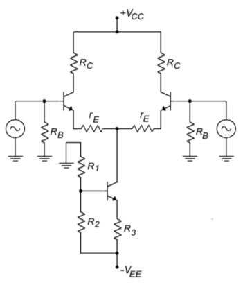
Figure \(\PageIndex{12}\): Improved current source.
The tail current is found by determining the potential across \(R_2\) and subtracting the 0.7 V \(V_{BE}\) drop. The remaining potential appears across \(R_3\). Given the voltage and resistance, Ohm’s Law will let you find the tail current. In this circuit, \(R_2\) is sometimes replaced with a Zener diode. This can help to reduce temperature induced current fluctuations. In any case, the effective resistance of this current source is considerably larger than the simple tail resistor variation. It is largely dependent on the characteristics of the tail current transistor, and can easily be in the megohm region.
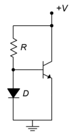
Figure \(\PageIndex{13}\): Current mirror.
1.6.5: Current Mirror
A very popular biasing technique in integrated circuits involves the current mirror. Current mirrors are also employed as active loads in order to optimize a circuit’s gain. A simple current mirror is shown in Figure \(\PageIndex{13}\). This circuit requires that the transconductance curves of the diode and the transistor be very closely matched. One way to guarantee this is to use two transistors, and form one of them into a diode by shorting its collector to its base. If we use an approximate forward bias potential of 0.7 V and ignore the small base current, the current through the diode is
\[ I_D = \frac{V_{CC}−0.7\ V}{R} \nonumber \]
In reality, the diode potential will probably not be exactly 0.7 V. This will have little effect on \(I_d\) though. Because the diode is in parallel with the transistor’s base-emitter junction, we know that \(V_d = V_{BE}\). If the two devices have identical transconductance curves, the transistor’s emitter current will equal the diode current. You can think of the transistor as mirroring the diode’s current, hence the circuit’s name. If the two device curves are slightly askew, then the two currents will not be identical. This is shown graphically in Figure \(\PageIndex{14}\).
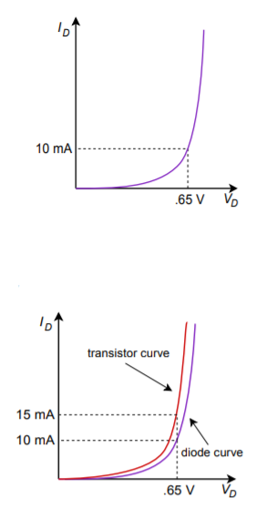
Figure \(\PageIndex{14}\): Transfer curve mismatch.
Example \(\PageIndex{3}\)
A current mirror could be used in the circuit of Figure \(\PageIndex{12}\). The result is shown in Figure \(\PageIndex{15}\). If the positive power supply is 15 V, the negative supply is -10 V, and \(R\) is 10 k\Omega, the tail current will be
\[ I_D = \frac{V_{CC} −V_{EE} −V_{D}}{R} \nonumber \]
\[ I_D = \frac{15\ V -(-10\ V) -0.7\ V}{10 k\Omega} \nonumber \]
\[ I_D = 2.43\ mA \nonumber \]
Because the tail current is the mirror current,
\[ I_T = I_D \nonumber \]
\[ I_T = 2.43\ mA \nonumber \]
Biasing of this type is very popular in operational amplifiers. Another use for current mirrors is in the application of active loads. Instead of using simple resistors for the collector loads, a current mirror may be used instead. A PNP based current mirror suitable for use as an active load in our previous circuits is shown in Figure \(\PageIndex{16}\).
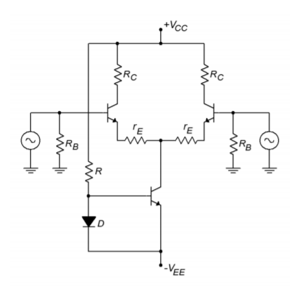
Figure \(\PageIndex{15}\): Current mirror bias.
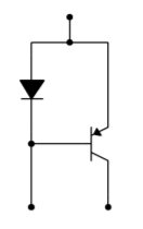
Figure \(\PageIndex{16}\): Active load current mirror.
To use this, we simply remove the two collector resistors from a circuit such as Figure \(\PageIndex{15}\), and drop in the current mirror. The result of this operation is shown in Figure \(\PageIndex{17}\). The current mirror active load produces a very high internal impedance, thus contributing to a very high differential gain. In effect, by using a constant current source in the collectors, all AC current is forced into the following stage. You may also note that the number of resistors used in the circuit has decreased considerably.
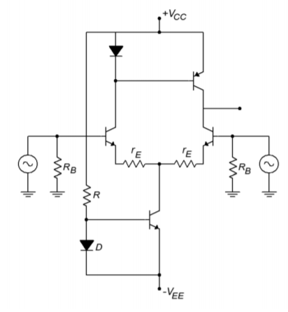
Figure \(\PageIndex{17}\): Current mirrors for bias and active load.