
10.4: Series Circuit Analysis
- Page ID
- 52956

\( \newcommand{\vecs}[1]{\overset { \scriptstyle \rightharpoonup} {\mathbf{#1}} } \)
\( \newcommand{\vecd}[1]{\overset{-\!-\!\rightharpoonup}{\vphantom{a}\smash {#1}}} \)
\( \newcommand{\dsum}{\displaystyle\sum\limits} \)
\( \newcommand{\dint}{\displaystyle\int\limits} \)
\( \newcommand{\dlim}{\displaystyle\lim\limits} \)
\( \newcommand{\id}{\mathrm{id}}\) \( \newcommand{\Span}{\mathrm{span}}\)
( \newcommand{\kernel}{\mathrm{null}\,}\) \( \newcommand{\range}{\mathrm{range}\,}\)
\( \newcommand{\RealPart}{\mathrm{Re}}\) \( \newcommand{\ImaginaryPart}{\mathrm{Im}}\)
\( \newcommand{\Argument}{\mathrm{Arg}}\) \( \newcommand{\norm}[1]{\| #1 \|}\)
\( \newcommand{\inner}[2]{\langle #1, #2 \rangle}\)
\( \newcommand{\Span}{\mathrm{span}}\)
\( \newcommand{\id}{\mathrm{id}}\)
\( \newcommand{\Span}{\mathrm{span}}\)
\( \newcommand{\kernel}{\mathrm{null}\,}\)
\( \newcommand{\range}{\mathrm{range}\,}\)
\( \newcommand{\RealPart}{\mathrm{Re}}\)
\( \newcommand{\ImaginaryPart}{\mathrm{Im}}\)
\( \newcommand{\Argument}{\mathrm{Arg}}\)
\( \newcommand{\norm}[1]{\| #1 \|}\)
\( \newcommand{\inner}[2]{\langle #1, #2 \rangle}\)
\( \newcommand{\Span}{\mathrm{span}}\) \( \newcommand{\AA}{\unicode[.8,0]{x212B}}\)
\( \newcommand{\vectorA}[1]{\vec{#1}} % arrow\)
\( \newcommand{\vectorAt}[1]{\vec{\text{#1}}} % arrow\)
\( \newcommand{\vectorB}[1]{\overset { \scriptstyle \rightharpoonup} {\mathbf{#1}} } \)
\( \newcommand{\vectorC}[1]{\textbf{#1}} \)
\( \newcommand{\vectorD}[1]{\overrightarrow{#1}} \)
\( \newcommand{\vectorDt}[1]{\overrightarrow{\text{#1}}} \)
\( \newcommand{\vectE}[1]{\overset{-\!-\!\rightharpoonup}{\vphantom{a}\smash{\mathbf {#1}}}} \)
\( \newcommand{\vecs}[1]{\overset { \scriptstyle \rightharpoonup} {\mathbf{#1}} } \)
\(\newcommand{\longvect}{\overrightarrow}\)
\( \newcommand{\vecd}[1]{\overset{-\!-\!\rightharpoonup}{\vphantom{a}\smash {#1}}} \)
\(\newcommand{\avec}{\mathbf a}\) \(\newcommand{\bvec}{\mathbf b}\) \(\newcommand{\cvec}{\mathbf c}\) \(\newcommand{\dvec}{\mathbf d}\) \(\newcommand{\dtil}{\widetilde{\mathbf d}}\) \(\newcommand{\evec}{\mathbf e}\) \(\newcommand{\fvec}{\mathbf f}\) \(\newcommand{\nvec}{\mathbf n}\) \(\newcommand{\pvec}{\mathbf p}\) \(\newcommand{\qvec}{\mathbf q}\) \(\newcommand{\svec}{\mathbf s}\) \(\newcommand{\tvec}{\mathbf t}\) \(\newcommand{\uvec}{\mathbf u}\) \(\newcommand{\vvec}{\mathbf v}\) \(\newcommand{\wvec}{\mathbf w}\) \(\newcommand{\xvec}{\mathbf x}\) \(\newcommand{\yvec}{\mathbf y}\) \(\newcommand{\zvec}{\mathbf z}\) \(\newcommand{\rvec}{\mathbf r}\) \(\newcommand{\mvec}{\mathbf m}\) \(\newcommand{\zerovec}{\mathbf 0}\) \(\newcommand{\onevec}{\mathbf 1}\) \(\newcommand{\real}{\mathbb R}\) \(\newcommand{\twovec}[2]{\left[\begin{array}{r}#1 \\ #2 \end{array}\right]}\) \(\newcommand{\ctwovec}[2]{\left[\begin{array}{c}#1 \\ #2 \end{array}\right]}\) \(\newcommand{\threevec}[3]{\left[\begin{array}{r}#1 \\ #2 \\ #3 \end{array}\right]}\) \(\newcommand{\cthreevec}[3]{\left[\begin{array}{c}#1 \\ #2 \\ #3 \end{array}\right]}\) \(\newcommand{\fourvec}[4]{\left[\begin{array}{r}#1 \\ #2 \\ #3 \\ #4 \end{array}\right]}\) \(\newcommand{\cfourvec}[4]{\left[\begin{array}{c}#1 \\ #2 \\ #3 \\ #4 \end{array}\right]}\) \(\newcommand{\fivevec}[5]{\left[\begin{array}{r}#1 \\ #2 \\ #3 \\ #4 \\ #5 \\ \end{array}\right]}\) \(\newcommand{\cfivevec}[5]{\left[\begin{array}{c}#1 \\ #2 \\ #3 \\ #4 \\ #5 \\ \end{array}\right]}\) \(\newcommand{\mattwo}[4]{\left[\begin{array}{rr}#1 \amp #2 \\ #3 \amp #4 \\ \end{array}\right]}\) \(\newcommand{\laspan}[1]{\text{Span}\{#1\}}\) \(\newcommand{\bcal}{\cal B}\) \(\newcommand{\ccal}{\cal C}\) \(\newcommand{\scal}{\cal S}\) \(\newcommand{\wcal}{\cal W}\) \(\newcommand{\ecal}{\cal E}\) \(\newcommand{\coords}[2]{\left\{#1\right\}_{#2}}\) \(\newcommand{\gray}[1]{\color{gray}{#1}}\) \(\newcommand{\lgray}[1]{\color{lightgray}{#1}}\) \(\newcommand{\rank}{\operatorname{rank}}\) \(\newcommand{\row}{\text{Row}}\) \(\newcommand{\col}{\text{Col}}\) \(\renewcommand{\row}{\text{Row}}\) \(\newcommand{\nul}{\text{Nul}}\) \(\newcommand{\var}{\text{Var}}\) \(\newcommand{\corr}{\text{corr}}\) \(\newcommand{\len}[1]{\left|#1\right|}\) \(\newcommand{\bbar}{\overline{\bvec}}\) \(\newcommand{\bhat}{\widehat{\bvec}}\) \(\newcommand{\bperp}{\bvec^\perp}\) \(\newcommand{\xhat}{\widehat{\xvec}}\) \(\newcommand{\vhat}{\widehat{\vvec}}\) \(\newcommand{\uhat}{\widehat{\uvec}}\) \(\newcommand{\what}{\widehat{\wvec}}\) \(\newcommand{\Sighat}{\widehat{\Sigma}}\) \(\newcommand{\lt}{<}\) \(\newcommand{\gt}{>}\) \(\newcommand{\amp}{&}\) \(\definecolor{fillinmathshade}{gray}{0.9}\)The techniques employed for series AC circuit analysis are the same as those used for DC. The key item to remember for series circuits, whether AC or DC, as that the current will be the same everywhere in a series connection. The major analysis tools are Ohm's law, Kirchhoff's voltage law (KVL), and optionally, the voltage divider rule.
KVL states that the sum of voltages around a loop must be zero, or that the sum of voltage rises around a loop must equal the sum of voltage drops:
\[\sum v \uparrow = \sum v \downarrow \label{2.2} \]
The voltage divider rule for AC states that the voltage across any component or group of components is proportional to the ratio of the impedance of said component and the total series impedance. For some component \(A\) driven by source \(e\),
\[v_A = e \frac{Z_A}{Z_{Total}} \label{2.3} \]
If current is the desired quantity, the equivalent impedance of the network is found and then divided into the equivalent source voltage. If the voltages across specific components are desired, they can be found using the circulating current and Ohm's law. Alternately, they can be computed using the voltage divider rule. If a current source is driving the series circuit then the circulating current is the source current. Individual component voltages may be found using the source current and Ohm's law. The source voltage may be found by summing the component voltages via KVL, or by determining the equivalent series impedance and multiplying it by the source current.
Example \(\PageIndex{1}\)
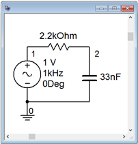
For the circuit of Figure \(\PageIndex{1}\), find the circulating current and the voltages across the capacitor and resistor.
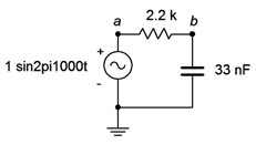
The first step is to determine \(X_C\) and then find \(Z_{total}\). Then use Ohm's law to find the circulating current.
\[X_C =− j \frac{1}{2\pi f C} \nonumber \]
\[X_C = − j \frac{1}{2\pi 1000Hz 33nF} \nonumber \]
\[X_C =− j 4823 \Omega \nonumber \]
\[Z_{Total} = R+(− j X_C ) \nonumber \]
\[Z_{Total} = 2200 \Omega − j 4823 \Omega \nonumber \]
\[Z_{Total} = 5301\angle −65.5^{\circ} \Omega \nonumber \]
\[i = \frac{v}{Z} \nonumber \]
\[i = \frac{1V}{5301\angle −65.5^{\circ} \Omega} \nonumber \]
\[i = 188.6\angle 65.5^{\circ} \mu A \nonumber \]
Now use Ohm's law to find the component voltages.
\[v_R = i\times R \nonumber \]
\[v_R = 188.6\angle 65.5^{\circ} \mu A\times 2200\angle 0^{\circ} \Omega \nonumber \]
\[v_R = 0.4149\angle 65.5^{\circ} V \nonumber \]
\[v_C = i\times X_C \nonumber \]
\[v_C = 188.6\angle 65.5^{\circ} \mu A\times 4823\angle −90^{\circ} \Omega \nonumber \]
\[v_C = 0.9098\angle −24.5^{\circ} V \nonumber \]
To complete this Example, we shall generate a series of plots: First off, an impedance plot showing the vector combination of \(R\) and \(X_C\) leading to \(Z_{Total}\). This is shown in Figure \(\PageIndex{2}\).
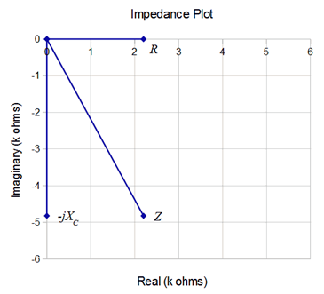
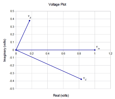
Next, Figure \(\PageIndex{3}\) illustrates the phasor diagram of the three voltages. It may not be immediately apparent but an examination of this plot shows that it is just a counterclockwise rotation of the impedance plot. In fact, it is rotated by 65.5 degrees, the phase angle of the current. This should come as no surprise as the current is multiplied by each resistance, reactance or impedance to develop the voltage, and a vector multiplication simply adds the angles.
Also, note that if we simply summed the magnitudes of the component voltages, the result would be considerably larger than the input voltage, seeming to violate KVL. In contrast, once a proper vector summation is performed, all is right in paradise.
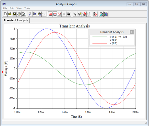
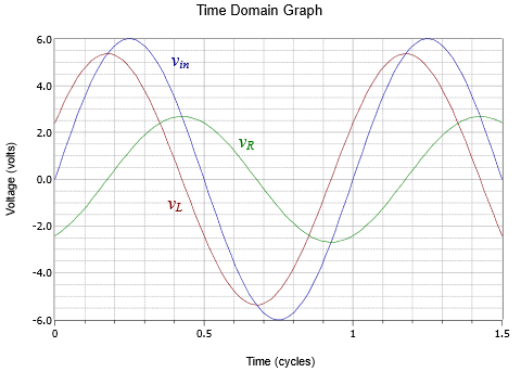
For further clarity, Figure \(\PageIndex{4}\) plots the voltages in the time domain. Note how the component voltages add graphically resulting in the input voltage.
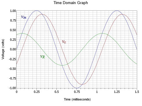
The time shifts may be computed for verification as follows:
\[\theta = 360^{\circ} \frac{\Delta t}{T} \nonumber \]
\[\Delta t_R = T \frac{\theta_R}{360^{\circ}} \nonumber \]
\[\Delta t_R = 1 ms \frac{65.5^{\circ}}{360^{\circ}} \nonumber \]
\[\Delta t_R = 181.9\mu s \nonumber \]
\[\Delta t_C = T \frac{\theta_C}{360^{\circ}} \nonumber \]
\[\Delta t_C = 1ms \frac{−24.5^{\circ}}{360^{\circ}} \nonumber \]
\[\Delta t_C =−68\mu s \nonumber \]
Thus we verify the resistor voltage leading (to the left) by 181.9 \(\mu\)s and the capacitor voltage lagging (to the right) by 68 \(\mu\)s, as seen in Figure \(\PageIndex{4}\).
Computer Simulation
The circuit of Example \(\PageIndex{1}\) is captured into a simulator as shown in Figure \(\PageIndex{5}\). Node voltage 1 corresponds to the input voltage and node 2 corresponds to the capacitor voltage. The resistor voltage is merely the difference between these two, or node 1 minus node 2.
A transient or time domain simulation is performed. The results of the simulation are shown in Figure \(\PageIndex{6}\). Note the tight agreement with the computed results as plotted in Figure \(\PageIndex{4}\).
We will now examine a variety of different series circuits. To ease the computations, we will simply state values for the component reactances rather than specify a frequency along with inductor and/or capacitor values.
Example \(\PageIndex{2}\)
Determine the component voltages for the circuit shown in Figure \(\PageIndex{7}\).
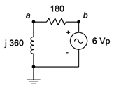
Given the reference direction of the source (which produces a counterclockwise reference current), the voltage across the resistor will be defined as \(v_b − v_a\). The first step is to find the equivalent series impedance. By inspection, this is \(180 + j360 \Omega\), which is equivalent to \(402.5\angle 63.4^{\circ} \Omega\).
The voltages can be found via the voltage divider rule.
\[v_L = e \frac{X_L}{Z} \nonumber \]
\[v_L = 6\angle 0^{\circ} V \frac{360\angle 90^{\circ} \Omega}{ 402.5\angle 63.4^{\circ} \Omega} \nonumber \]
\[v_L = 5.366\angle 26.6^{\circ} Vp \nonumber \]
\[v_R = e \frac{R}{Z} \nonumber \]
\[v_R = 6\angle 0^{\circ} V \frac{180\angle 0^{\circ} \Omega}{402.5\angle 63.4 ^{\circ} \Omega} \nonumber \]
\[v_R = 2.683\angle −63.4^{\circ} Vp \nonumber \]
The rectangular versions of \(v_L\) and \(v_R\) are \(4.8 + j2.4\) and \(1.2 − j2.4\) respectively, summing up to the source of \(6\angle 0^{\circ}\). This is illustrated in the phasor voltage plot of Figure \(\PageIndex{8}\).
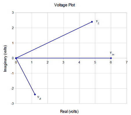
Compare the plot of Figure \(\PageIndex{8}\) to that of the RC circuit in Figure \(\PageIndex{3}\). In this circuit, the impedance is inductive. This causes the current to lag the voltage, the opposite of the case for the RC circuit. Thus, the resistor voltage winds up below the real axis instead of above it (remember, the current and voltage for a resistor are in phase, and therefore the voltage across the resistor will have the same phase angle as the current through it). Once again, simply summing the magnitudes of the voltages yields a greater value than the source, however, a proper vector addition shows that KVL is satisfied.
A time domain plot of the source and component voltages is shown in Figure \(\PageIndex{9}\). Note the similarity with the plot of Figure \(\PageIndex{4}\). Further, note how the time positions of the component voltages have swapped.
Finally, as a source frequency was not specified for this circuit, the time scale of Figure \(\PageIndex{9}\) is calibrated in terms of cycles rather than seconds.
Example \(\PageIndex{3}\)
Find the voltages \(v_a\) and \(v_b\) in the circuit of Figure \(\PageIndex{10}\). Assume the current source is the reference of \(0^{\circ}\).
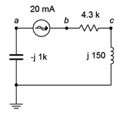
Ohm's law may be used directly as the current is set by the source. Given the reference direction of the 20 mA source, the reference polarity for the capacitor voltage will be + to − from bottom to top. Thus, \(v_a\) is negative.
\[v_a = v_C = −i\times X_C \nonumber \]
\[v_a =−20E-3\angle 0^{\circ} A\times 1000\angle −90^{\circ} \Omega \nonumber \]
\[v_a =−20\angle −90^{\circ} V \nonumber \]
Recalling that a negative magnitude is the same as a \(180^{\circ}\) phase shift, we may remove the magnitude's negative sign by adding \(180^{\circ}\) to the phase angle. Therefore, \(v_a\) may also be written as \(20\angle 90^{\circ}\).
The node \(b\) voltage is found by multiplying the current by the impedance seen from node \(b\) to ground.
\[v_b = i\times (R+jX_L ) \nonumber \]
\[v_b = 20 \angle 0^{\circ} mA\times (4300+j 150\Omega ) \nonumber \]
\[v_b = 86.05\angle 2^{\circ} V \nonumber \]
Notice the small size of the phase angle. This is expected given that the inductive reactance is so much smaller than the resistive component. Finally, these voltage are RMS as the current is assumed to be RMS (not having been labeled as peak or peak-to-peak).
Example \(\PageIndex{4}\)
Find the voltage \(v_{bd}\) in the circuit of Figure \(\PageIndex{11}\). \(E_1 = 2\angle 0^{\circ}\) volts peak and \(E_2 = 5\angle 60^{\circ}\) volts peak.
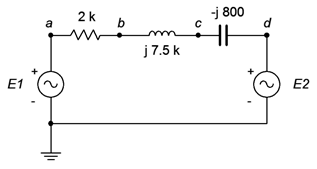
The first step is to find the equivalent source voltage. Voltage sources in series add, however, note the reference polarity for \(E_2\). If we take \(E_1\) as the system reference, then the combined source is \(E_1 − E_2\). Using \(E_1\) as the reference source creates a clockwise reference current and thus a positive reference polarity for \(v_{bd}\). If \(E_2\) was taken as the reference then \(v_{bd}\) would be assumed to be negative due to the assumed counterclockwise reference direction of the resulting current. Either way will work.
\[E_{Total} = E_1 −E_2 \nonumber \]
\[E_{Total} = 2\angle 0^{\circ} Vp −5\angle 60 ^{\circ} Vp \nonumber \]
\[E_{Total} = 4.359\angle −96.6^{\circ} Vp \nonumber \]
We can now use a voltage divider between the impedance seen from node \(b\) to node \(d\) versus the total series impedance. The impedance of the circuit is \(2 k + j7.5 k − j800 \Omega\), or \(2 k + j6.7 k \Omega\). This is equivalent to \(6992\angle 73.4^{\circ} \Omega\). The impedance of between nodes \(b\) and \(d\) is \(j7.5 k − j800 \Omega\), or \(j6.7 k \Omega\). In polar form this is \(6700\angle 90^{\circ} \Omega\).
The voltage divider yields:
\[v_{bd} = e \frac{Z_{bd}}{Z_{Total}} \nonumber \]
\[v_{bd} = 4.359\angle −96.6^{\circ} V \frac{6700\angle 90^{\circ} \Omega}{6992\angle 73.4 ^{\circ} \Omega} \nonumber \]
\[v_{bd} = 4.177\angle −80^{\circ} Vp \nonumber \]
Although we have answered the question, at this point attempting to visualize the waveforms in your head to verify the results may be a little challenging. No problem! If we also find the voltage across the resistor, we can check to see if KVL is verified using a phasor diagram. First, the resistor voltage may be found using the voltage divider rule.
\[v_R = e \frac{R}{Z_{Total}} \nonumber \]
\[v_R = 4.359\angle −96.6^{\circ} V \frac{2000\angle 0^{\circ} \Omega}{6992\angle 73.4^{\circ} \Omega} \nonumber \]
\[v_R =1.247\angle −170^{\circ} Vp \nonumber \]
We now plot all four voltages as seen in Figure \(\PageIndex{12}\) (note the unequal horizontal versus vertical scaling for ease of visual analysis).
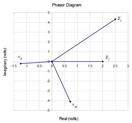
KVL tells us that the sum of the voltage rises must equal the sum of the voltage drops. We had used \(E_1\) as the reference and treated it as a rise. This made the reference direction clockwise for the circulating current. As a consequence, \(v_R\) and \(v_{bd}\) are voltage drops. \(E_2\) is also seen as a drop given its reference polarity markings. In other words, \(E_1\) should equal the sum of \(v_R\), \(v_{bd}\) and \(E_2\). Let's see if this is borne out graphically in the phasor diagram.
Looking at imaginary parts first, \(E_1\) is strictly real so the other three vectors should sum to zero for their imaginary parts. The imaginary part of \(E_2\) is about +4.3 while the other two come in around −4.1 and −0.2, so they do balance. For the real parts, \(E_2\) is +2.5, \(v_{bd}\) is about +0.7 and \(v_R\) is about −1.2. These add up to +2, the real component of \(E_1\). Everything balances. For more exacting results, you could convert each of the polar form results into rectangular form and add the reals to the reals, and the imaginaries to the imaginaries, and get the same result. In fact, using the prior recorded values, the three drops sum to \(1.997\angle 0.0013^{\circ}\) volts versus precisely \(2\angle 0^{\circ}\) volts. This small deviation is due to the accumulated rounding and truncation errors of the intermediate results.
Sometimes a problem concerns determining resistance or reactance values. The solution paths will require use of the analysis rules in reverse. For example, if a resistor value is needed to set a specific current, the total required impedance can be determined from this current and the given voltage supply. The values of the other series components can then be subtracted from the total (using rectangular form), yielding the required resistor or reactance value.
Another possibility is determining a specific capacitance or inductance to meet certain requirements. An example of this would be a simple crossover network for a loudspeaker system. Generally, a single transducer is incapable of reproducing music signals of all frequencies at sufficiently loud levels while maintaining low distortion. Consequently, the frequency range is split into two or more bands with each being covered by a transducer optimized to reproduce those frequencies. These transducers, along with a few electrical components, are then packaged into an appropriate enclosure commonly referred to as a loudspeaker1. In a basic system, the audible spectrum is split into two parts, as seen in Figure \(\PageIndex{13}\). The low frequencies are handled by a large transducer called a woofer, while the high frequencies are handled by a small, light transducer called a tweeter that can follow the rapidly changing high frequency content with accuracy. Woofers are not capable of reproducing high frequencies, and excessive low frequency content can physically damage a tweeter. Thus, some means of “steering” the high frequency content to the tweeter and the low frequency content to the woofer must be employed. One way to do this is to place an inductor or capacitor in series with the transducer.
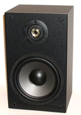
Figure \(\PageIndex{14}\) shows a simple way to block low frequencies from a tweeter. In this diagram, the loudspeaker is modeled as a resistor. Although this is not perfectly accurate, it is sufficient to illustrate the idea.
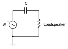
To understand this concept, simply think of the circuit as a voltage divider between the loudspeaker and the reactance of the capacitor. Capacitive reactance is inversely proportional to frequency. The circuit is designed such that \(X_C\) is much larger than than the impedance of the loudspeaker at very low frequencies. This means that very little of a low frequency signal will reach the loudspeaker as most of that voltage will drop across the capacitor. In contrast, at high frequencies \(X_C\) is much smaller than the tweeter's impedance and thus virtually all of the source signal reaches the loudspeaker. The transition point between these two regions is called the crossover frequency and is usually defined as the point where \(X_C\) equals the magnitude of the loudspeaker impedance. For a woofer, the capacitor would be replaced by an inductor. At low frequencies the inductive reactance would be minimal, thereby allowing all of the low frequency content to reach the woofer. The opposite happens at high frequencies. The inductive reactance would rise with frequency and eventually prevent or “choke off” the signal to the woofer (hence, the slang term “choke” for an inductor).
Example \(\PageIndex{5}\)
Referring to the circuit of Figure \(\PageIndex{14}\), assume the loudspeaker impedance is \(8\angle 0^{\circ} \Omega\). Determine a capacitor value for a crossover frequency of 2.5 kHz. At this frequency the magnitude of \(X_C\) should be the same as that of the loudspeaker. For a 10 volt RMS input signal, determine the loudspeaker voltage at frequencies of 100 Hz, 2.5 kHz and 15 kHz.
The first step is to determine the value of the capacitor such that at 2.5 kHz \(X_C\) equals \(8 \Omega\). To do this, simply rearrange the capacitive reactance formula:
\[X_C = − j \frac{1}{2 \pi f C} \nonumber \]
\[C = {1}{2\pi f | X_C |} \nonumber \]
\[C = \frac{1}{2\pi 2500Hz 8\Omega} \nonumber \]
\[C = 7.96\mu F \nonumber \]
To find the loudspeaker voltage at the three specified frequencies, first find the reactance at that frequency and then use the voltage divider rule. We already know that at 2.5 kHz the reactance is \(−j8 \Omega\).
\[v_{loudspeaker} = e \frac{Z_{Load}}{Z_{Total}} \nonumber \]
\[v_{loudspeaker}= 10 \angle 0^{\circ} Vrms \frac{8\Omega}{8 − j 8\Omega} \nonumber \]
\[v_{loudspeaker} = 7.07\angle 45 ^{\circ} Vrms \nonumber \]
At 100 Hz, the frequency has decreased by a factor of 25 so the reactance goes up by the same factor yielding \(−j200 \Omega\).
\[v_{loudspeaker} = e \frac{Z_{Load}}{Z_{Total}} \nonumber \]
\[v_{loudspeaker} = 10 \angle 0^{\circ} Vrms \frac{8\Omega}{8 − j 200 \Omega} \nonumber \]
\[v_{loudspeaker} = 0.4\angle 87.7^{\circ} Vrms \nonumber \]
At 15 kHz, the frequency has increased by a factor of 6 so the reactance goes down by the same factor yielding \(−j1.333 \Omega\).
\[v_{loudspeaker} = e \frac{Z_{Load}}{Z_{Total}} \nonumber \]
\[v_{loudspeaker} = 10 \angle 0^{\circ} Vrms \frac{8\Omega}{8 − j 1.333\Omega} \nonumber \]
\[v_{loudspeaker} = 9.86\angle 9.5^{\circ} Vrms \nonumber \]
From this tally, it should be obvious that the lowest bass frequencies will experience attenuation while the highest frequencies will see little reduction in amplitude. This is just what we want.
The concept of a variation in output voltage with respect to frequency, or frequency response, will be examined in much greater detail in upcoming chapters.
References
1To add some confusion, the term “loudspeaker” can refer to either the individual transducers (engineer-speak) or the entire finished system (audiophile-speak).