3.4.10: CMOS Logic
- Page ID
- 89977

\( \newcommand{\vecs}[1]{\overset { \scriptstyle \rightharpoonup} {\mathbf{#1}} } \)
\( \newcommand{\vecd}[1]{\overset{-\!-\!\rightharpoonup}{\vphantom{a}\smash {#1}}} \)
\( \newcommand{\dsum}{\displaystyle\sum\limits} \)
\( \newcommand{\dint}{\displaystyle\int\limits} \)
\( \newcommand{\dlim}{\displaystyle\lim\limits} \)
\( \newcommand{\id}{\mathrm{id}}\) \( \newcommand{\Span}{\mathrm{span}}\)
( \newcommand{\kernel}{\mathrm{null}\,}\) \( \newcommand{\range}{\mathrm{range}\,}\)
\( \newcommand{\RealPart}{\mathrm{Re}}\) \( \newcommand{\ImaginaryPart}{\mathrm{Im}}\)
\( \newcommand{\Argument}{\mathrm{Arg}}\) \( \newcommand{\norm}[1]{\| #1 \|}\)
\( \newcommand{\inner}[2]{\langle #1, #2 \rangle}\)
\( \newcommand{\Span}{\mathrm{span}}\)
\( \newcommand{\id}{\mathrm{id}}\)
\( \newcommand{\Span}{\mathrm{span}}\)
\( \newcommand{\kernel}{\mathrm{null}\,}\)
\( \newcommand{\range}{\mathrm{range}\,}\)
\( \newcommand{\RealPart}{\mathrm{Re}}\)
\( \newcommand{\ImaginaryPart}{\mathrm{Im}}\)
\( \newcommand{\Argument}{\mathrm{Arg}}\)
\( \newcommand{\norm}[1]{\| #1 \|}\)
\( \newcommand{\inner}[2]{\langle #1, #2 \rangle}\)
\( \newcommand{\Span}{\mathrm{span}}\) \( \newcommand{\AA}{\unicode[.8,0]{x212B}}\)
\( \newcommand{\vectorA}[1]{\vec{#1}} % arrow\)
\( \newcommand{\vectorAt}[1]{\vec{\text{#1}}} % arrow\)
\( \newcommand{\vectorB}[1]{\overset { \scriptstyle \rightharpoonup} {\mathbf{#1}} } \)
\( \newcommand{\vectorC}[1]{\textbf{#1}} \)
\( \newcommand{\vectorD}[1]{\overrightarrow{#1}} \)
\( \newcommand{\vectorDt}[1]{\overrightarrow{\text{#1}}} \)
\( \newcommand{\vectE}[1]{\overset{-\!-\!\rightharpoonup}{\vphantom{a}\smash{\mathbf {#1}}}} \)
\( \newcommand{\vecs}[1]{\overset { \scriptstyle \rightharpoonup} {\mathbf{#1}} } \)
\(\newcommand{\longvect}{\overrightarrow}\)
\( \newcommand{\vecd}[1]{\overset{-\!-\!\rightharpoonup}{\vphantom{a}\smash {#1}}} \)
\(\newcommand{\avec}{\mathbf a}\) \(\newcommand{\bvec}{\mathbf b}\) \(\newcommand{\cvec}{\mathbf c}\) \(\newcommand{\dvec}{\mathbf d}\) \(\newcommand{\dtil}{\widetilde{\mathbf d}}\) \(\newcommand{\evec}{\mathbf e}\) \(\newcommand{\fvec}{\mathbf f}\) \(\newcommand{\nvec}{\mathbf n}\) \(\newcommand{\pvec}{\mathbf p}\) \(\newcommand{\qvec}{\mathbf q}\) \(\newcommand{\svec}{\mathbf s}\) \(\newcommand{\tvec}{\mathbf t}\) \(\newcommand{\uvec}{\mathbf u}\) \(\newcommand{\vvec}{\mathbf v}\) \(\newcommand{\wvec}{\mathbf w}\) \(\newcommand{\xvec}{\mathbf x}\) \(\newcommand{\yvec}{\mathbf y}\) \(\newcommand{\zvec}{\mathbf z}\) \(\newcommand{\rvec}{\mathbf r}\) \(\newcommand{\mvec}{\mathbf m}\) \(\newcommand{\zerovec}{\mathbf 0}\) \(\newcommand{\onevec}{\mathbf 1}\) \(\newcommand{\real}{\mathbb R}\) \(\newcommand{\twovec}[2]{\left[\begin{array}{r}#1 \\ #2 \end{array}\right]}\) \(\newcommand{\ctwovec}[2]{\left[\begin{array}{c}#1 \\ #2 \end{array}\right]}\) \(\newcommand{\threevec}[3]{\left[\begin{array}{r}#1 \\ #2 \\ #3 \end{array}\right]}\) \(\newcommand{\cthreevec}[3]{\left[\begin{array}{c}#1 \\ #2 \\ #3 \end{array}\right]}\) \(\newcommand{\fourvec}[4]{\left[\begin{array}{r}#1 \\ #2 \\ #3 \\ #4 \end{array}\right]}\) \(\newcommand{\cfourvec}[4]{\left[\begin{array}{c}#1 \\ #2 \\ #3 \\ #4 \end{array}\right]}\) \(\newcommand{\fivevec}[5]{\left[\begin{array}{r}#1 \\ #2 \\ #3 \\ #4 \\ #5 \\ \end{array}\right]}\) \(\newcommand{\cfivevec}[5]{\left[\begin{array}{c}#1 \\ #2 \\ #3 \\ #4 \\ #5 \\ \end{array}\right]}\) \(\newcommand{\mattwo}[4]{\left[\begin{array}{rr}#1 \amp #2 \\ #3 \amp #4 \\ \end{array}\right]}\) \(\newcommand{\laspan}[1]{\text{Span}\{#1\}}\) \(\newcommand{\bcal}{\cal B}\) \(\newcommand{\ccal}{\cal C}\) \(\newcommand{\scal}{\cal S}\) \(\newcommand{\wcal}{\cal W}\) \(\newcommand{\ecal}{\cal E}\) \(\newcommand{\coords}[2]{\left\{#1\right\}_{#2}}\) \(\newcommand{\gray}[1]{\color{gray}{#1}}\) \(\newcommand{\lgray}[1]{\color{lightgray}{#1}}\) \(\newcommand{\rank}{\operatorname{rank}}\) \(\newcommand{\row}{\text{Row}}\) \(\newcommand{\col}{\text{Col}}\) \(\renewcommand{\row}{\text{Row}}\) \(\newcommand{\nul}{\text{Nul}}\) \(\newcommand{\var}{\text{Var}}\) \(\newcommand{\corr}{\text{corr}}\) \(\newcommand{\len}[1]{\left|#1\right|}\) \(\newcommand{\bbar}{\overline{\bvec}}\) \(\newcommand{\bhat}{\widehat{\bvec}}\) \(\newcommand{\bperp}{\bvec^\perp}\) \(\newcommand{\xhat}{\widehat{\xvec}}\) \(\newcommand{\vhat}{\widehat{\vvec}}\) \(\newcommand{\uhat}{\widehat{\uvec}}\) \(\newcommand{\what}{\widehat{\wvec}}\) \(\newcommand{\Sighat}{\widehat{\Sigma}}\) \(\newcommand{\lt}{<}\) \(\newcommand{\gt}{>}\) \(\newcommand{\amp}{&}\) \(\definecolor{fillinmathshade}{gray}{0.9}\)Consider the following, shown in Figure \(\PageIndex{1}\).
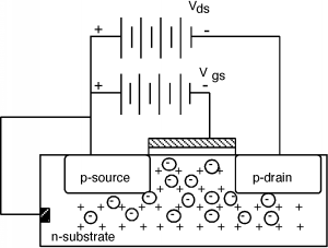
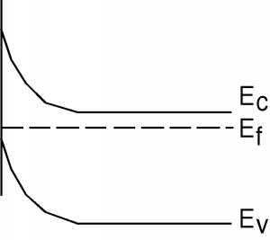
This looks a lot like our previous MOSFET except that now we have an n-type substrate and the source and drain regions are p-type. If we apply a negative \(V_{\text{gs}}\) (with the source connected to the n-type substrate) then the induced negative charge on the gate will drive away the electrons, and if the bands under the gate are bent up sufficiently, form an inversion layer of holes (see Figure \(\PageIndex{2}\), thus making an enhancement mode p-channel MOSFET, or a PMOS transistor. (As opposed to an NMOS transistor which we studied first.). Note that a PMOS transistor will have a negative \(V_{t}\). That is, the gate voltage has to be less than the source/substrate voltage in order to turn the device on. The more negative \(V_{\text{gs}}\) is, the more current we will have flowing through the device.
It turns out that a combination of both an n-channel and a p-channel device on the same circuit can be very advantageous. Such technology is called CMOS, for "complementary MOS". Here is how we use a p-channel transistor in the inverter circuit.
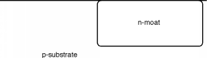
First of all, however, we have to see how we would make one. There is a fundamental problem in trying to use both n-channel and p-channel devices in the same circuit. What is it? It would seem we need two different kinds of substrates, both a p-type substrate for the n-channel transistor, and an n-type substrate for the p-channel device. There is a way around this problem by making what is called a tank or a moat. A moat is a relatively deep region of one type of material placed into a host substrate of the opposite type (Figure \(\PageIndex{3}\)). We can put n-type source/drain regions into the p-substrate and p-type source/drain regions into the n-moat. In Figure \(\PageIndex{4}\), we will also show the gates, and how the whole inverter is connected together.


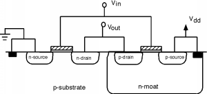
Now let's draw the schematic: A p-channel device is drawn just like an n-channel device, except we put a little "bubble" on the gate to signify that it is a MOSFET of a different color. Although we usually don't do this all the time, we have also shown the substrate connections in this diagram. These connections show that a MOSFET is at least a four-terminal device, not a three-terminal one as people often assume. Since, in a p-channel device, the substrate is n-type, we show the substrate connection as an outward pointing arrow. The p-type substrate for the n-channel device is shown as an inward pointing arrow. The n-channel substrate is connected to ground, and the p-channel substrate is connected to \(V_{\text{dd}}\). Note that since the n-moat is at \(V_{\text{dd}}\) and the p-substrate is at ground, the moat-substrate p-n junction is reverse biased, and so no current should flow between them.
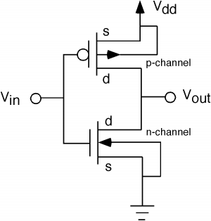
We usually do not label the source and drain either, but we do here, just for completeness. Note that unlike the bipolar transistor, the FET is truly a symmetric device. There is really no way to tell the source from the drain. By convention, we call the element which is connected to the substrate (or moat) the source, and the other the drain. You will sometimes hear the region under the gate (either substrate or moat) referred to as the backbody.
Now let's see how this circuit works. If \(V_{\text{in}}\) is high (at or near \(V_{\text{dd}}\)) the NMOS transistor will be turned on. The voltage between the gate and substrate of the p-channel device is at or near zero. The gate is at \(V_{\text{dd}}\) and so is the moat! Hence the upper transistor will be turned off. The output will thus be low.
If the input voltage is at or near ground (a "low") then the n-channel device is turned off. The voltage between the gate and substrate of the p-channel device is now \(\simeq \left( -V_{\text{dd}} \right)\). (The gate is \(\simeq 0\) and the substrate is at \(V_{\text{dd}}\).) If the PMOS transistor has a threshold voltage \(V_{t}\) of, say, \(-2 \mathrm{~V}\), then it will be turned on and the output will be high. Note however, that in either state, high or low, there is no static current flowing through the inverter.
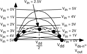
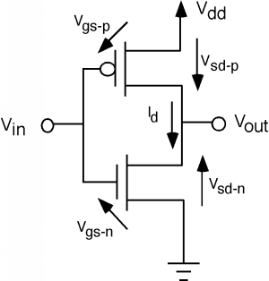
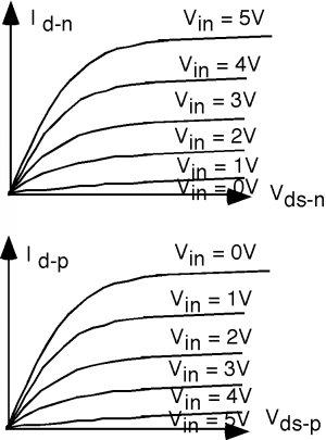
The transfer characteristics for this circuit are a little more complicated. First, let's make sure we have our voltages and currents defined. From Figure \(\PageIndex{6}\), the n-channel gate-source voltage, \(V_{\text{gs-}n}\), is just \(V_{\text{in}}\). The gate-source voltage for the p-channel device, \(V_{\text{gs-}p}\), is \(V_{\text{in}} - V_{\text{dd}\); \(V_{\text{ds-}p}\), the drain-source voltage for the p-channel transistor can be written as \(V_{\text{ds-}n} - V_{\text{dd}}\). For current, \(I_{d \text{-} n} = I_{d \text{-} p} = I_{d}\). As seen in Figure \(\PageIndex{7}\), we have two sets of characteristic curves. Note that since \(V_{\text{gs-}p} = V_{\text{in}} - V_{\text{dd}}\), when \(V_{\text{in}} = 0 \mathrm{~V}\), \(V_{\text{gs-}p} = -5 \mathrm{~V}\) and so the transistor is strongly turned on.
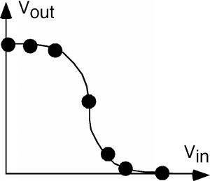
We have a number of different "load lines" in this case, because for each \(V_{\text{in}}\) we have a different curve for both the n- and p-channel transistors. This is shown in Figure \(\PageIndex{8}\). The black spots show the point of intersection. Follow a few of the curves along to see if you agree with where the spots have been placed. We have also added a pair of dotted curves for \(V_{\text{in}} = 2.5 \mathrm{~V}\) so we can get the "turn-over" point. Projecting the location of the black dots to the \(V_{\text{ds-}n}\) (or \(V_{\text{out}}\)) axis will gives us a value for \(V_{\text{out}}\) for each of the input voltages, \(V_{\text{in}}\). The resulting curve is shown in Figure \(\PageIndex{9}\). This gives us a good "feel" for how the inverter works, and how the output varies with the input. Note that this transfer curve is quite symmetric about 2.5 volts, and goes all the way from +5 to 0 volts on the output.