
3.3.2: Introduction to Semiconductors
- Page ID
- 89947

\( \newcommand{\vecs}[1]{\overset { \scriptstyle \rightharpoonup} {\mathbf{#1}} } \)
\( \newcommand{\vecd}[1]{\overset{-\!-\!\rightharpoonup}{\vphantom{a}\smash {#1}}} \)
\( \newcommand{\dsum}{\displaystyle\sum\limits} \)
\( \newcommand{\dint}{\displaystyle\int\limits} \)
\( \newcommand{\dlim}{\displaystyle\lim\limits} \)
\( \newcommand{\id}{\mathrm{id}}\) \( \newcommand{\Span}{\mathrm{span}}\)
( \newcommand{\kernel}{\mathrm{null}\,}\) \( \newcommand{\range}{\mathrm{range}\,}\)
\( \newcommand{\RealPart}{\mathrm{Re}}\) \( \newcommand{\ImaginaryPart}{\mathrm{Im}}\)
\( \newcommand{\Argument}{\mathrm{Arg}}\) \( \newcommand{\norm}[1]{\| #1 \|}\)
\( \newcommand{\inner}[2]{\langle #1, #2 \rangle}\)
\( \newcommand{\Span}{\mathrm{span}}\)
\( \newcommand{\id}{\mathrm{id}}\)
\( \newcommand{\Span}{\mathrm{span}}\)
\( \newcommand{\kernel}{\mathrm{null}\,}\)
\( \newcommand{\range}{\mathrm{range}\,}\)
\( \newcommand{\RealPart}{\mathrm{Re}}\)
\( \newcommand{\ImaginaryPart}{\mathrm{Im}}\)
\( \newcommand{\Argument}{\mathrm{Arg}}\)
\( \newcommand{\norm}[1]{\| #1 \|}\)
\( \newcommand{\inner}[2]{\langle #1, #2 \rangle}\)
\( \newcommand{\Span}{\mathrm{span}}\) \( \newcommand{\AA}{\unicode[.8,0]{x212B}}\)
\( \newcommand{\vectorA}[1]{\vec{#1}} % arrow\)
\( \newcommand{\vectorAt}[1]{\vec{\text{#1}}} % arrow\)
\( \newcommand{\vectorB}[1]{\overset { \scriptstyle \rightharpoonup} {\mathbf{#1}} } \)
\( \newcommand{\vectorC}[1]{\textbf{#1}} \)
\( \newcommand{\vectorD}[1]{\overrightarrow{#1}} \)
\( \newcommand{\vectorDt}[1]{\overrightarrow{\text{#1}}} \)
\( \newcommand{\vectE}[1]{\overset{-\!-\!\rightharpoonup}{\vphantom{a}\smash{\mathbf {#1}}}} \)
\( \newcommand{\vecs}[1]{\overset { \scriptstyle \rightharpoonup} {\mathbf{#1}} } \)
\(\newcommand{\longvect}{\overrightarrow}\)
\( \newcommand{\vecd}[1]{\overset{-\!-\!\rightharpoonup}{\vphantom{a}\smash {#1}}} \)
\(\newcommand{\avec}{\mathbf a}\) \(\newcommand{\bvec}{\mathbf b}\) \(\newcommand{\cvec}{\mathbf c}\) \(\newcommand{\dvec}{\mathbf d}\) \(\newcommand{\dtil}{\widetilde{\mathbf d}}\) \(\newcommand{\evec}{\mathbf e}\) \(\newcommand{\fvec}{\mathbf f}\) \(\newcommand{\nvec}{\mathbf n}\) \(\newcommand{\pvec}{\mathbf p}\) \(\newcommand{\qvec}{\mathbf q}\) \(\newcommand{\svec}{\mathbf s}\) \(\newcommand{\tvec}{\mathbf t}\) \(\newcommand{\uvec}{\mathbf u}\) \(\newcommand{\vvec}{\mathbf v}\) \(\newcommand{\wvec}{\mathbf w}\) \(\newcommand{\xvec}{\mathbf x}\) \(\newcommand{\yvec}{\mathbf y}\) \(\newcommand{\zvec}{\mathbf z}\) \(\newcommand{\rvec}{\mathbf r}\) \(\newcommand{\mvec}{\mathbf m}\) \(\newcommand{\zerovec}{\mathbf 0}\) \(\newcommand{\onevec}{\mathbf 1}\) \(\newcommand{\real}{\mathbb R}\) \(\newcommand{\twovec}[2]{\left[\begin{array}{r}#1 \\ #2 \end{array}\right]}\) \(\newcommand{\ctwovec}[2]{\left[\begin{array}{c}#1 \\ #2 \end{array}\right]}\) \(\newcommand{\threevec}[3]{\left[\begin{array}{r}#1 \\ #2 \\ #3 \end{array}\right]}\) \(\newcommand{\cthreevec}[3]{\left[\begin{array}{c}#1 \\ #2 \\ #3 \end{array}\right]}\) \(\newcommand{\fourvec}[4]{\left[\begin{array}{r}#1 \\ #2 \\ #3 \\ #4 \end{array}\right]}\) \(\newcommand{\cfourvec}[4]{\left[\begin{array}{c}#1 \\ #2 \\ #3 \\ #4 \end{array}\right]}\) \(\newcommand{\fivevec}[5]{\left[\begin{array}{r}#1 \\ #2 \\ #3 \\ #4 \\ #5 \\ \end{array}\right]}\) \(\newcommand{\cfivevec}[5]{\left[\begin{array}{c}#1 \\ #2 \\ #3 \\ #4 \\ #5 \\ \end{array}\right]}\) \(\newcommand{\mattwo}[4]{\left[\begin{array}{rr}#1 \amp #2 \\ #3 \amp #4 \\ \end{array}\right]}\) \(\newcommand{\laspan}[1]{\text{Span}\{#1\}}\) \(\newcommand{\bcal}{\cal B}\) \(\newcommand{\ccal}{\cal C}\) \(\newcommand{\scal}{\cal S}\) \(\newcommand{\wcal}{\cal W}\) \(\newcommand{\ecal}{\cal E}\) \(\newcommand{\coords}[2]{\left\{#1\right\}_{#2}}\) \(\newcommand{\gray}[1]{\color{gray}{#1}}\) \(\newcommand{\lgray}[1]{\color{lightgray}{#1}}\) \(\newcommand{\rank}{\operatorname{rank}}\) \(\newcommand{\row}{\text{Row}}\) \(\newcommand{\col}{\text{Col}}\) \(\renewcommand{\row}{\text{Row}}\) \(\newcommand{\nul}{\text{Nul}}\) \(\newcommand{\var}{\text{Var}}\) \(\newcommand{\corr}{\text{corr}}\) \(\newcommand{\len}[1]{\left|#1\right|}\) \(\newcommand{\bbar}{\overline{\bvec}}\) \(\newcommand{\bhat}{\widehat{\bvec}}\) \(\newcommand{\bperp}{\bvec^\perp}\) \(\newcommand{\xhat}{\widehat{\xvec}}\) \(\newcommand{\vhat}{\widehat{\vvec}}\) \(\newcommand{\uhat}{\widehat{\uvec}}\) \(\newcommand{\what}{\widehat{\wvec}}\) \(\newcommand{\Sighat}{\widehat{\Sigma}}\) \(\newcommand{\lt}{<}\) \(\newcommand{\gt}{>}\) \(\newcommand{\amp}{&}\) \(\definecolor{fillinmathshade}{gray}{0.9}\)Page by:
If we only had to worry about simple conductors, life would not be very complicated, but on the other hand we wouldn't be able to make computers, cell phones, and a lot of other things which we have found to be useful. We will now move on, and talk about another class of conductors called semiconductors.
In order to understand semiconductors and in fact to get a more accurate picture of how metals, or normal conductors actually work, we really have to resort to quantum mechanics. Electrons in a solid are very tiny objects, and it turns out that when things get small enough, they no longer exactly follow the classical "Newtonian" laws of physics that we are all familiar with from everyday experience. It is not the purpose of this course to teach you quantum mechanics, so what we are going to do instead is describe the results which come from looking at the behavior of electrons in a solid from a quantum mechanical point of view.
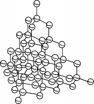
Solids (at least the ones we will be talking about, and especially semiconductors) are crystalline materials, which means that they have their atoms arranged in a ordered fashion. We can take silicon (the most important semiconductor) as an example. Silicon is a group IV element, which means it has four electrons in its outer or valence shell. Silicon crystallizes in a structure called the diamond crystal lattice. This is shown in Figure \(\PageIndex{1}\). Each silicon atom has four covalent bonds, arranged in a tetrahedral formation about the atom center.
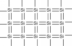
In two dimensions, we can schematically represent a piece of single-crystal silicon as shown in Figure \(\PageIndex{2}\). Each silicon atom shares its four valence electrons with valence electrons from four nearest neighbors, filling the shell to 8 electrons, and forming a stable, periodic structure. Once the atoms have been arranged like this, the outer valence electrons are no longer strongly bound to the host atom. The outer shells of all of the atoms blend together and form what is called a band. The electrons are now free to move about within this band, and this can lead to electrical conductivity as we discussed earlier.
This is not the complete story, however, for it turns out that due to quantum mechanical effects, there is not just one band which holds electrons, but several of them. What will follow is a very qualitative picture of how the electrons are distributed when they are in a periodic solid, and there are necessarily some details which we will be forced to gloss over. On the other hand, this will give you a pretty good picture of what is going on, and may enable you to have some understanding of how a semiconductor really works. Electrons are not only distributed throughout the solid crystal spatially, but they also have a distribution in energy as well. The potential energy function within the solid is periodic in nature. This potential function comes from the positively charged atomic nuclei which are arranged in the crystal in a regular array. A detailed analysis of how electron wave functions, the mathematical abstraction which one must use to describe how small quantum mechanical objects behave when they are in a periodic potential, gives rise to an energy distribution somewhat like that shown in Figure \(\PageIndex{3}\).
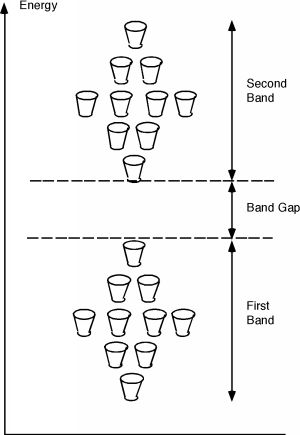
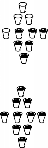
Firstly, unlike the case for free electrons, in a periodic solid, electrons are not free to take on any energy value they wish. They are forced into specific energy levels called allowed states which are represented by the cups in the figure. The allowed states are not distributed uniformly in energy either. They are grouped into specific configurations called energy bands. There are no allowed levels at zero energy and for some distance above that. Moving up from zero energy, we then encounter the first energy band. At the bottom of the band there are very few allowed states, but as we move up in energy, the number of allowed states first increases, and then falls off again. We then come to a region with no allowed states, called an energy band gap. Above the band gap, another band of allowed states exists. This goes on and on, with any given material having many such bands and band gaps. This situation is shown schematically in Figure \(\PageIndex{3}\), where the small cups represent allowed energy levels, and the vertical axis represents electron energy.
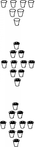
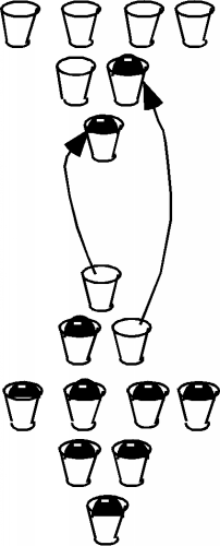
It turns out that each band has exactly \(2N\) allowed states in it, where \(N\) is the total number of atoms in the particular crystal sample we are talking about. (Since there are 10 cups in each band in the figure, it must represent a crystal with just 5 atoms in it. Not a very big crystal at all!) Into these bands we must now distribute all of the valence electrons associated with the atoms, with the restriction that we can only put one electron into each allowed state. (This is the result of something called the Pauli exclusion principle.) Since in the case of silicon there are 4 valence electrons per atom, we would just fill up the first two bands, and the next would be empty. (If we make the logical assumption that the electrons will fill in the levels with the lowest energy first, and only go into higher lying levels if the ones below are already filled.) This situation is shown in Figure \(\PageIndex{4}\).
Here, we have represented electrons as small black balls with a "-" sign on them. Indeed, the first two bands are completely full, and the next is empty. What will happen if we apply an electric field to the sample of silicon? Remember that the diagram we have at hand right now is an energy based one; we are showing how the electrons are distributed in energy, not how they are arranged spatially. On this diagram we cannot show how they will move about, but only how they will change their energy as a result of the applied field. The electric field will exert a force on the electrons and attempt to accelerate them. If the electrons are accelerated, then they must increase their kinetic energy. Unfortunately, there are no empty allowed states in either of the filled bands. An electron would have to jump all the way up into the next (empty) band in order to take on more energy. In silicon, the gap between the top of the highest most occupied band and the lowest unoccupied band is \(1.1 \mathrm{~eV}\). (One \(\mathrm{eV}\) is the potential energy gained by an electron moving across an electrical potential of one volt.) The mean free path or distance over which an electron would normally move before it suffers a collision is about 30 nm \( \left( \simeq \left( 300 \times 10^{-8} \right) \mathrm{~cm} \right)\) and so you would need a very large electric field (several hundred thousand \(\frac{\mathrm{volts}}{\mathrm{cm}}\)) in order for the electron to pick up enough energy to "jump the gap". This makes it appear that silicon would be a very bad conductor of electricity, and in fact, very pure silicon is very poor electrical conductor.
Some semiconductors, such as Gallium Arsenide, are such poor conductors that very pure material is sometimes called "semi-insulating." Insulators, such as quartz ( crystalline silicon dioxide) or diamond (crystalline carbon) have such large band gaps that it is extremely rare for an electron to gain enough energy to jump the gap.
A metal is an element with a very small band gap, or even overlapping bands. In effect, a metal ends up with an upper band which is partially full of electrons. This is illustrated in Figure \(\PageIndex{5}\) Here we see that one band is full, and the next is just half full. This would be the situation for the Group III element aluminum, for instance. If we apply an electric field to these carriers, those near the top of the distribution can indeed move into higher energy levels by acquiring a small kinetic energy of motion, and easily move from one place to the next. In reality, the whole situation is a bit more complex than we have shown here, but this is not too far from how it actually works.
So, back to our silicon sample. If there are no places for electrons to "move" into, then how does silicon work as a "semiconductor"? Well, in the first place, it turns out that not all of the electrons are in the bottom two bands. In silicon, unlike say, quartz or diamond, the band gap between the topmost full band and the next empty one is not so large. As we mentioned above, it is only about \(1.1 \mathrm{~eV}\). So long as the silicon is not at absolute zero temperature, some electrons near the top of the full band can acquire enough thermal energy that they can "hop" the gap, and end up in the upper band, called the conduction band. This situation is shown in Figure \(\PageIndex{6}\).
In silicon at room temperature, roughly \(10^{10}\) electrons per cubic centimeter are thermally excited across the band-gap at any one time. It should be noted that the excitation process is a continuous one. Electrons are being excited across the band, but then they fall back down into empty spots in the lower band. On average, however, the \(10^{10}\) in each \(\mathrm{cm}^{3}\)