
Electron-Hole Recombination
- Page ID
- 323
\( \newcommand{\vecs}[1]{\overset { \scriptstyle \rightharpoonup} {\mathbf{#1}} } \)
\( \newcommand{\vecd}[1]{\overset{-\!-\!\rightharpoonup}{\vphantom{a}\smash {#1}}} \)
\( \newcommand{\dsum}{\displaystyle\sum\limits} \)
\( \newcommand{\dint}{\displaystyle\int\limits} \)
\( \newcommand{\dlim}{\displaystyle\lim\limits} \)
\( \newcommand{\id}{\mathrm{id}}\) \( \newcommand{\Span}{\mathrm{span}}\)
( \newcommand{\kernel}{\mathrm{null}\,}\) \( \newcommand{\range}{\mathrm{range}\,}\)
\( \newcommand{\RealPart}{\mathrm{Re}}\) \( \newcommand{\ImaginaryPart}{\mathrm{Im}}\)
\( \newcommand{\Argument}{\mathrm{Arg}}\) \( \newcommand{\norm}[1]{\| #1 \|}\)
\( \newcommand{\inner}[2]{\langle #1, #2 \rangle}\)
\( \newcommand{\Span}{\mathrm{span}}\)
\( \newcommand{\id}{\mathrm{id}}\)
\( \newcommand{\Span}{\mathrm{span}}\)
\( \newcommand{\kernel}{\mathrm{null}\,}\)
\( \newcommand{\range}{\mathrm{range}\,}\)
\( \newcommand{\RealPart}{\mathrm{Re}}\)
\( \newcommand{\ImaginaryPart}{\mathrm{Im}}\)
\( \newcommand{\Argument}{\mathrm{Arg}}\)
\( \newcommand{\norm}[1]{\| #1 \|}\)
\( \newcommand{\inner}[2]{\langle #1, #2 \rangle}\)
\( \newcommand{\Span}{\mathrm{span}}\) \( \newcommand{\AA}{\unicode[.8,0]{x212B}}\)
\( \newcommand{\vectorA}[1]{\vec{#1}} % arrow\)
\( \newcommand{\vectorAt}[1]{\vec{\text{#1}}} % arrow\)
\( \newcommand{\vectorB}[1]{\overset { \scriptstyle \rightharpoonup} {\mathbf{#1}} } \)
\( \newcommand{\vectorC}[1]{\textbf{#1}} \)
\( \newcommand{\vectorD}[1]{\overrightarrow{#1}} \)
\( \newcommand{\vectorDt}[1]{\overrightarrow{\text{#1}}} \)
\( \newcommand{\vectE}[1]{\overset{-\!-\!\rightharpoonup}{\vphantom{a}\smash{\mathbf {#1}}}} \)
\( \newcommand{\vecs}[1]{\overset { \scriptstyle \rightharpoonup} {\mathbf{#1}} } \)
\(\newcommand{\longvect}{\overrightarrow}\)
\( \newcommand{\vecd}[1]{\overset{-\!-\!\rightharpoonup}{\vphantom{a}\smash {#1}}} \)
\(\newcommand{\avec}{\mathbf a}\) \(\newcommand{\bvec}{\mathbf b}\) \(\newcommand{\cvec}{\mathbf c}\) \(\newcommand{\dvec}{\mathbf d}\) \(\newcommand{\dtil}{\widetilde{\mathbf d}}\) \(\newcommand{\evec}{\mathbf e}\) \(\newcommand{\fvec}{\mathbf f}\) \(\newcommand{\nvec}{\mathbf n}\) \(\newcommand{\pvec}{\mathbf p}\) \(\newcommand{\qvec}{\mathbf q}\) \(\newcommand{\svec}{\mathbf s}\) \(\newcommand{\tvec}{\mathbf t}\) \(\newcommand{\uvec}{\mathbf u}\) \(\newcommand{\vvec}{\mathbf v}\) \(\newcommand{\wvec}{\mathbf w}\) \(\newcommand{\xvec}{\mathbf x}\) \(\newcommand{\yvec}{\mathbf y}\) \(\newcommand{\zvec}{\mathbf z}\) \(\newcommand{\rvec}{\mathbf r}\) \(\newcommand{\mvec}{\mathbf m}\) \(\newcommand{\zerovec}{\mathbf 0}\) \(\newcommand{\onevec}{\mathbf 1}\) \(\newcommand{\real}{\mathbb R}\) \(\newcommand{\twovec}[2]{\left[\begin{array}{r}#1 \\ #2 \end{array}\right]}\) \(\newcommand{\ctwovec}[2]{\left[\begin{array}{c}#1 \\ #2 \end{array}\right]}\) \(\newcommand{\threevec}[3]{\left[\begin{array}{r}#1 \\ #2 \\ #3 \end{array}\right]}\) \(\newcommand{\cthreevec}[3]{\left[\begin{array}{c}#1 \\ #2 \\ #3 \end{array}\right]}\) \(\newcommand{\fourvec}[4]{\left[\begin{array}{r}#1 \\ #2 \\ #3 \\ #4 \end{array}\right]}\) \(\newcommand{\cfourvec}[4]{\left[\begin{array}{c}#1 \\ #2 \\ #3 \\ #4 \end{array}\right]}\) \(\newcommand{\fivevec}[5]{\left[\begin{array}{r}#1 \\ #2 \\ #3 \\ #4 \\ #5 \\ \end{array}\right]}\) \(\newcommand{\cfivevec}[5]{\left[\begin{array}{c}#1 \\ #2 \\ #3 \\ #4 \\ #5 \\ \end{array}\right]}\) \(\newcommand{\mattwo}[4]{\left[\begin{array}{rr}#1 \amp #2 \\ #3 \amp #4 \\ \end{array}\right]}\) \(\newcommand{\laspan}[1]{\text{Span}\{#1\}}\) \(\newcommand{\bcal}{\cal B}\) \(\newcommand{\ccal}{\cal C}\) \(\newcommand{\scal}{\cal S}\) \(\newcommand{\wcal}{\cal W}\) \(\newcommand{\ecal}{\cal E}\) \(\newcommand{\coords}[2]{\left\{#1\right\}_{#2}}\) \(\newcommand{\gray}[1]{\color{gray}{#1}}\) \(\newcommand{\lgray}[1]{\color{lightgray}{#1}}\) \(\newcommand{\rank}{\operatorname{rank}}\) \(\newcommand{\row}{\text{Row}}\) \(\newcommand{\col}{\text{Col}}\) \(\renewcommand{\row}{\text{Row}}\) \(\newcommand{\nul}{\text{Nul}}\) \(\newcommand{\var}{\text{Var}}\) \(\newcommand{\corr}{\text{corr}}\) \(\newcommand{\len}[1]{\left|#1\right|}\) \(\newcommand{\bbar}{\overline{\bvec}}\) \(\newcommand{\bhat}{\widehat{\bvec}}\) \(\newcommand{\bperp}{\bvec^\perp}\) \(\newcommand{\xhat}{\widehat{\xvec}}\) \(\newcommand{\vhat}{\widehat{\vvec}}\) \(\newcommand{\uhat}{\widehat{\uvec}}\) \(\newcommand{\what}{\widehat{\wvec}}\) \(\newcommand{\Sighat}{\widehat{\Sigma}}\) \(\newcommand{\lt}{<}\) \(\newcommand{\gt}{>}\) \(\newcommand{\amp}{&}\) \(\definecolor{fillinmathshade}{gray}{0.9}\)Recombination is the mechanism that is utilized by extrinsic semiconductors to equilibrate excess charge carriers through the bringing together and annihilation of oppositely charged carriers. Specifically the annihilation of positively charged holes and negatively charged impurity or free electrons. Recombination results in the release of energy, this energy stems from the act of electrons jumping down from the conduction band in order to recombine with holes generated in the valence band. The energy released can be in the form of photons or thermal lattice vibrations known as phonons. The resultant energy strength and type are determined by material characteristic band gap energy and the presence of defects within a material that can act as traps for charge carrier movement. Understanding the distinction and controlling the dominating recombination mechanisms for materials is highly important for the optimization of semiconductor devices such as solar cells and light emitting diodes.
Introduction
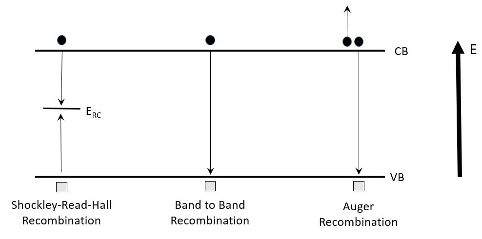
When a free electron inhabits the conduction band, it exists in a meta-stable state. Therefore to compensate for the unfavorable energy state the electron will move into an empty state, characterized as an electron hole. The movement of the electron into the empty state can occur in one or more steps through the band gap. The difference in energies between the meta-stable and the final state of the electron is then released so to allow the electron to occupy its final state. The process of electron and hole annihilation is known as recombination. If the energy released through recombination is in the form of a photon, the process is known as radiative-recombination and is most common for electrons moving fully from the conduction to the valence band. Non-radiative recombination is often the result of material defects and intermediate energy levels in the band gap. Non-radiative recombination can be categorized as either Auger or defect level driven recombination.
Radiative Recombination
Radiative recombination is the mechanism responsible for photoemission in semiconductor light emitting diodes and is mainly associated with band to band recombination as a result of the high energy differences associated with a complete band gap transition. Direct band to band recombination is only possible in materials with extremely low defect concentrations due to the fact that strain fields in the crystal structure will alter atomic interaction distances and strengths. This difference is directly related to electron interaction density in the material which, according to the band theory of semiconductors, will alter the band structure of the material. Direct band gap Extrinsic semiconductors, like GaAs, are manufactured to have little to no crystalline defects so to prevent the creation of defect levels within the band gap.
When radiative recombination occurs, the photon emitted has a characteristic energy similar to the band gap of the material and therefore will have a very weak interaction with the material. Therefore allowing for photons emitted within the sample through radiative recombination events to escape.
Non-Radiative Recombination
When intermediate energy levels are introduced into the band gap of a material through defects in the crystal structure, charge carriers have the possibility of becoming trapped, thus making recombination extremely less favorable. When an electron or a hole is captured in an energy level close to the conduction or valence bands respectively, it is said that the carrier is trapped. The probabilities for electron occupation and hole occupation are represented by equations one and two respectively. For an electron trap, the energy required for an electron to occupy that energy state is significantly higher than the chance for a hole to occupy said state (Eqn.3).
\[\sigma_n * e^{\frac{-E_t * N}{K_B * T}} \label{1}\]
The converse is true for a hole trap (Eqn.4).
\[\sigma_p * N_{t n} * V_{t h} \label{2}\]
As a result of this disparity in occupation of a state, specific to one type of charge carrier, the trapped carrier will not be able to recombine and eventually return to the initial state. A high concentration of carrier traps will result in the reduction in carrier mobility and in turn a reduction in recombination rate.
\[\sigma_n \gg \sigma_p \label{3}\]
\[\sigma_n \ll \sigma_p \label{4}\]

Energy levels present within the band gap with energies that are located more equidistant from both the valence and conduction bands are known as recombination centers. After a carrier is captured by a recombination center there is a finite probability that a carrier of opposite charge will also be capable of occupying the same energy state, therefore resulting an an electron-hole pair annihilation. This form of recombination is known as Shockley-Read-Hall (SRH) or defect level recombination. The resultant intermediate step results in a lower energy difference between the starting and ending energies of the electron and in turn a smaller energy released during recombination. This energy is often in the form of thermal vibrations known as phonons, which are then absorbed into the material which results in heating. This heating occurs at the defect sites within the material and can be extremely detrimental to device efficiency due to the fact that electron mobility decreases with phonon concentration and that heat energy can result in growth of strained areas within the material.
Auger recombination requires the interaction of three carriers. when an electron and a hole interact and recombine the energy is not transferred into heat energy or thermal vibrations. Instead the energy is transferred into an electron within the conduction band, which is then promoted to an energy higher in the conduction band. This electron then releases energy in the form of thermal vibrations as it returns to the lowest possible state within the conduction band. For this reason Auger recombination is highly detrimental to the efficiency of extrinsic semiconductor LED's with high concentrations of electron donor atoms. Additionally, the concentration of Auger recombination events increases with an increase in input energy intensity as a result an increased electron concentration in the conduction band.
Gallium Nitride LED's
Gallium nitride (GaN) is a direct band gap binary III/V semiconductor that is commonly used for bright light emitting diodes. It is also commonly used for solar cells in military and space applications as a result of its low sensitivity to ionizing radiation. GaN has a wide band gap of 3.4 eV which allows for the emission of violet light [3]. This violet emission is used in Blu-Ray players to read disks. Gallium nitride LEDs can be manufactured to produce light with colors ranging from the low end of visible up to ultraviolet. This is done by altering the concentrations and types of dopant atoms.
Pure GaN is highly crystalline with a wurtzite crystal structure. When dopant atoms are added to make the semiconductor either p-type (addition of magnesium) or n-type(addition of Si or oxygen), the material exhibits a high dislocation density. This high dislocation density, on the order of ten billion defects per square centimeter introduced tensile stresses making the semiconductors brittle and inefficient [4]. The inefficiency stemmed from a high number of non-radiative recombination centers where strain fields absorbed energy and released it as phonons into the material. The addition of buffer layers when depositing the GaN using molecular beam epitaxy at low temperatures allowed for the relaxation of the stresses and in turn a high performance LED. The ability to alter the size of the band gap for GaN while maintaining a low defect density led to the commercialization of light emmiting diodes of multiple colors and intensities. All as a result of reducing the number of defects and in turn the number of non-radiative recombination zones.
Questions
- Thin film crystalline GaN LEDs are grown on insulating substrates so to prevent current leakage, often there is a high lattice mismatch between the film and the substrate so intermediate layers are grown to reduce the amount of stress dislocations in the film. Why is the replication of defects in semiconductor thin films undesirable?
- A solar cell made of a heavily dosed silicon based semiconductor with no observed defects begins to experience a reduction in efficiency. What could be a potential cause for this reduced efficiency, and what is one practical solution to this problem?
- An orange colored LED is dipped in liquid nitrogen and then illuminated, a change to green, a smaller wavelength of light, was seen. Given that no defects were introduced, what is happening to the band to band recombination?
Answers
- Dislocations and other defects in the crystal structure of a extrinsic semiconductor like GaN will alter the band structure and possibly introduce non-radiative recombination centers, thus decreasing the LED efficiency and output.
- Materials with high concentrations of electrons in the conduction band are subject to Auger recombination regardless of defect presence. either choosing a different material with a lower electron donor concentration or by reducing the energy input you will lower the probability for Auger recombination and in turn increase efficiency of the solar cell.
- The electron interaction in the material is changing and in this case, results in the increased size of the band gap. Therefore the electrons have a higher difference in initial and final states, thus creating higher energy photons.
References
- Shockley, W.; Read, W. T. (1 September 1952). "Statistics of the Recombinations of Holes and Electrons". Physical Review 87 (5): 835–842. doi:10.1103/PhysRev.87.835.
- Honsberg, Christina, and Stuart Bowden. "Types of Recombination." Types of Recombination. PV Education, n.d. Web. 04 Dec. 2015. <www.pveducation.org/pvcdrom/p...-recombination>.
- Sugahara, Tomoya, Hisao Sato, Maosheng Hao, Yoshiki Naoi, Satoshi Kurai, Satoru Tottori, Kenji Yamashita, Katsushi Nishino, Linda T. Romano, and Shiro Sakai. "Direct Evidence That Dislocations Are Non-Radiative Recombination Centers in GaN." Jpn. J. Appl. Phys. Japanese Journal of Applied Physics 37.Part 2, No. 4A (1998): n. pag. IOP Science. Web. 07 Dec. 2015.