
8.5: Thermoelectric Effects
- Page ID
- 18987

\( \newcommand{\vecs}[1]{\overset { \scriptstyle \rightharpoonup} {\mathbf{#1}} } \)
\( \newcommand{\vecd}[1]{\overset{-\!-\!\rightharpoonup}{\vphantom{a}\smash {#1}}} \)
\( \newcommand{\dsum}{\displaystyle\sum\limits} \)
\( \newcommand{\dint}{\displaystyle\int\limits} \)
\( \newcommand{\dlim}{\displaystyle\lim\limits} \)
\( \newcommand{\id}{\mathrm{id}}\) \( \newcommand{\Span}{\mathrm{span}}\)
( \newcommand{\kernel}{\mathrm{null}\,}\) \( \newcommand{\range}{\mathrm{range}\,}\)
\( \newcommand{\RealPart}{\mathrm{Re}}\) \( \newcommand{\ImaginaryPart}{\mathrm{Im}}\)
\( \newcommand{\Argument}{\mathrm{Arg}}\) \( \newcommand{\norm}[1]{\| #1 \|}\)
\( \newcommand{\inner}[2]{\langle #1, #2 \rangle}\)
\( \newcommand{\Span}{\mathrm{span}}\)
\( \newcommand{\id}{\mathrm{id}}\)
\( \newcommand{\Span}{\mathrm{span}}\)
\( \newcommand{\kernel}{\mathrm{null}\,}\)
\( \newcommand{\range}{\mathrm{range}\,}\)
\( \newcommand{\RealPart}{\mathrm{Re}}\)
\( \newcommand{\ImaginaryPart}{\mathrm{Im}}\)
\( \newcommand{\Argument}{\mathrm{Arg}}\)
\( \newcommand{\norm}[1]{\| #1 \|}\)
\( \newcommand{\inner}[2]{\langle #1, #2 \rangle}\)
\( \newcommand{\Span}{\mathrm{span}}\) \( \newcommand{\AA}{\unicode[.8,0]{x212B}}\)
\( \newcommand{\vectorA}[1]{\vec{#1}} % arrow\)
\( \newcommand{\vectorAt}[1]{\vec{\text{#1}}} % arrow\)
\( \newcommand{\vectorB}[1]{\overset { \scriptstyle \rightharpoonup} {\mathbf{#1}} } \)
\( \newcommand{\vectorC}[1]{\textbf{#1}} \)
\( \newcommand{\vectorD}[1]{\overrightarrow{#1}} \)
\( \newcommand{\vectorDt}[1]{\overrightarrow{\text{#1}}} \)
\( \newcommand{\vectE}[1]{\overset{-\!-\!\rightharpoonup}{\vphantom{a}\smash{\mathbf {#1}}}} \)
\( \newcommand{\vecs}[1]{\overset { \scriptstyle \rightharpoonup} {\mathbf{#1}} } \)
\(\newcommand{\longvect}{\overrightarrow}\)
\( \newcommand{\vecd}[1]{\overset{-\!-\!\rightharpoonup}{\vphantom{a}\smash {#1}}} \)
\(\newcommand{\avec}{\mathbf a}\) \(\newcommand{\bvec}{\mathbf b}\) \(\newcommand{\cvec}{\mathbf c}\) \(\newcommand{\dvec}{\mathbf d}\) \(\newcommand{\dtil}{\widetilde{\mathbf d}}\) \(\newcommand{\evec}{\mathbf e}\) \(\newcommand{\fvec}{\mathbf f}\) \(\newcommand{\nvec}{\mathbf n}\) \(\newcommand{\pvec}{\mathbf p}\) \(\newcommand{\qvec}{\mathbf q}\) \(\newcommand{\svec}{\mathbf s}\) \(\newcommand{\tvec}{\mathbf t}\) \(\newcommand{\uvec}{\mathbf u}\) \(\newcommand{\vvec}{\mathbf v}\) \(\newcommand{\wvec}{\mathbf w}\) \(\newcommand{\xvec}{\mathbf x}\) \(\newcommand{\yvec}{\mathbf y}\) \(\newcommand{\zvec}{\mathbf z}\) \(\newcommand{\rvec}{\mathbf r}\) \(\newcommand{\mvec}{\mathbf m}\) \(\newcommand{\zerovec}{\mathbf 0}\) \(\newcommand{\onevec}{\mathbf 1}\) \(\newcommand{\real}{\mathbb R}\) \(\newcommand{\twovec}[2]{\left[\begin{array}{r}#1 \\ #2 \end{array}\right]}\) \(\newcommand{\ctwovec}[2]{\left[\begin{array}{c}#1 \\ #2 \end{array}\right]}\) \(\newcommand{\threevec}[3]{\left[\begin{array}{r}#1 \\ #2 \\ #3 \end{array}\right]}\) \(\newcommand{\cthreevec}[3]{\left[\begin{array}{c}#1 \\ #2 \\ #3 \end{array}\right]}\) \(\newcommand{\fourvec}[4]{\left[\begin{array}{r}#1 \\ #2 \\ #3 \\ #4 \end{array}\right]}\) \(\newcommand{\cfourvec}[4]{\left[\begin{array}{c}#1 \\ #2 \\ #3 \\ #4 \end{array}\right]}\) \(\newcommand{\fivevec}[5]{\left[\begin{array}{r}#1 \\ #2 \\ #3 \\ #4 \\ #5 \\ \end{array}\right]}\) \(\newcommand{\cfivevec}[5]{\left[\begin{array}{c}#1 \\ #2 \\ #3 \\ #4 \\ #5 \\ \end{array}\right]}\) \(\newcommand{\mattwo}[4]{\left[\begin{array}{rr}#1 \amp #2 \\ #3 \amp #4 \\ \end{array}\right]}\) \(\newcommand{\laspan}[1]{\text{Span}\{#1\}}\) \(\newcommand{\bcal}{\cal B}\) \(\newcommand{\ccal}{\cal C}\) \(\newcommand{\scal}{\cal S}\) \(\newcommand{\wcal}{\cal W}\) \(\newcommand{\ecal}{\cal E}\) \(\newcommand{\coords}[2]{\left\{#1\right\}_{#2}}\) \(\newcommand{\gray}[1]{\color{gray}{#1}}\) \(\newcommand{\lgray}[1]{\color{lightgray}{#1}}\) \(\newcommand{\rank}{\operatorname{rank}}\) \(\newcommand{\row}{\text{Row}}\) \(\newcommand{\col}{\text{Col}}\) \(\renewcommand{\row}{\text{Row}}\) \(\newcommand{\nul}{\text{Nul}}\) \(\newcommand{\var}{\text{Var}}\) \(\newcommand{\corr}{\text{corr}}\) \(\newcommand{\len}[1]{\left|#1\right|}\) \(\newcommand{\bbar}{\overline{\bvec}}\) \(\newcommand{\bhat}{\widehat{\bvec}}\) \(\newcommand{\bperp}{\bvec^\perp}\) \(\newcommand{\xhat}{\widehat{\xvec}}\) \(\newcommand{\vhat}{\widehat{\vvec}}\) \(\newcommand{\uhat}{\widehat{\uvec}}\) \(\newcommand{\what}{\widehat{\wvec}}\) \(\newcommand{\Sighat}{\widehat{\Sigma}}\) \(\newcommand{\lt}{<}\) \(\newcommand{\gt}{>}\) \(\newcommand{\amp}{&}\) \(\definecolor{fillinmathshade}{gray}{0.9}\)Three Related Effects
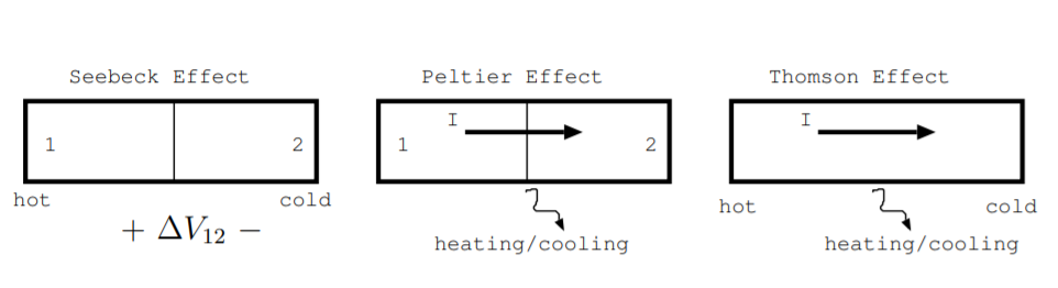
In the 1800s, three effects were experimentally observed. At first, it was not obvious that these experiments were related, but soon they were found to be three aspects of the same phenomenon [5, p. 113].
The first effect, now called the Seebeck effect, was discovered in 1821 by Thomas Seebeck [5, p. 113]. It is observed in a junction of two different metals or semiconductors. As discussed in Section 6.4, junctions are also used to make photovoltaic devices, LEDs, and semiconductor lasers. When the different sides of the junction are held at different temperatures, a voltage develops across the junction. The Seebeck coefficient \($\), in units \(\frac{V}{K}\), is defined as the ratio of that voltage to the temperature difference. More specifically, consider a junction where one side is held at a hotter temperature than the other, as shown in the left part of Fig. \(\PageIndex{1}\). The difference between the Seebeck coefficient in material one \($_1\) and the Seebeck coefficient in material two \($_2\) is given by the measured voltage across the junction \(\Delta V_{12}\) divided by the temperature difference between the materials \(\Delta T_{12}\) [110, p. 24].
\[$_1 - $_2 = \frac{\Delta V_{12}}{\Delta T_{12}} \nonumber \]
The difference between the Seebeck coefficients can be positive or negative because both the temperature difference and the measured voltage can be positive or negative. However, for any given material, the Seebeck coefficient is positive. To find the Seebeck coefficient for an unknown material, form a junction between that material and a material with known Seebeck coefficient, heat one end of the junction hotter than the other, and measure the voltage established. For most materials, the Seebeck coefficient is less than \(1 \frac{\mu V}{K}\). Some of the largest values of the Seebeck coefficient are found in materials containing tellurium. For example, (Bi\(_{0.7}\)Sb\(_{0.3})_2\) Te\(_3\) has \($ \approx 230 \frac{\mu V}{K} \)and PbTe has \($ \approx 400 \frac{\mu V}{K}\) [3].
To understand the physics behind the Seebeck effect, consider the flow of charges across this diode-like device. In metals, valence electrons are the charge carriers, and in semiconductors, both valence electrons and holes are the charge carriers. These charge carriers diffuse from the hot to the cold side of the junction. Consider a junction of two metals with no net charge on either side initially. If an electron moves from the hot side to the cold side, the hot side then will have a net positive charge, and the cold side will have a net negative charge. This movement of charges sets up an electric field and hence a voltage.
If we let the sample reach an equilibrium temperature, no voltage will be measured. A voltage is measured only during the time when charge carriers have diffused from one material to the other but when the material has not reached a uniform temperature. Thus, for a material to have a large thermoelectric effect, it must have a large electrical conductivity and small thermal conductivity. Thermoelectric devices are typically made from metals or semimetals because these materials satisfy this condition.
The second effect was discovered by Jean Peltier in 1834 [5, p. 113]. The Peltier effect is also observed in a junction of two different metals, semimetals, or semiconductors. It is illustrated in the middle part of Fig. \(\PageIndex{1}\). When a current, \(I\) in amperes, is supplied across a junction, heat is transferred. This effect occurs because charges from the supplied current flow through different materials with different thermal conductivities on the different sides of the junction. The effect is quantified by the Peltier coefficient for the junction, \(\displaystyle \prod_{12}\), or Peltier coefficients for the materials forming the junction, \(\displaystyle \prod_1\) and \(\displaystyle \prod_2\). More specifically, the Peltier coefficient is defined as
\[\prod_{12} = \prod_1 - \prod_2 = \frac{ \left( \frac{d\mathbb{Q}}{dt} \right) }{I} \nonumber \]
in the units of volts [110, p. 24]. The term \(\frac{d\mathbb{Q}}{dt}\) represents the rate heat is transferred in \(\frac{J}{s}\), and it may be positive or negative because the thermal conductivity in the first material may be higher or lower than in the second material. The Seebeck coefficient and the Peltier coefficient are related by
\[\prod_1 - \prod_2 = ($_1 - $_2)T. \nonumber \]
PbTe is a material with a relatively high Seebeck coefficient. At room temperature, it has coefficients \($ = 400 \frac{\mu V}{K}\) and
\[\prod = 400 \frac{\mu V}{K} \cdot 300K = 0.12V. \nonumber \]
The third effect was first discovered by William Thomson in the 1860s [3]. Thomson also derived the relationship between these three effects. It is illustrated on the right part of Fig. \(\PageIndex{1}\). When a current passes through a uniform piece of material which has a temperature gradient, heating or cooling will occur, and this result is known as the Thomson effect [3, p. 148] [110, p. 24] [5, p. 115]. To observe this effect, apply a temperature gradient across a piece of metal or semiconductor and also apply a current through the length of the material. Heating or cooling can be measured, and this effect is described by another coefficient. The Thomson coefficient \(\tau\) also has units \(\frac{V}{K}\). It is defined as the rate of heat generated over the product of the current and temperature difference.
\[ \tau = \frac {\frac {d\mathbb{Q}} {dt}} {I(T_h-T_c)} \nonumber \]
The Thomson and Seebeck coefficients for a single material are related by
\[\int_{0}^{T} \frac{\tau}{T^{\prime}} d T^{\prime}=$ \nonumber \]
where the integral is over temperature [110, p. 24].
These effects work both ways. We can use the Peltier effect, for example, to make either a heating or a cooling device. We can supply a current across a junction to produce a temperature differential, or we can supply a temperature difference to generate a current. All three effects relate to the fact that when the electrical conductivity is larger than the thermal conductivity, energy can be converted between a temperature differential and electricity. As an aside, materials with low electrical conductivity and high thermal conductivity are also used to make energy conversion devices. Components of motors and generators are often made from layers of metal and dielectrics with these properties [111, ch. 8].
Electrical Conductivity
Electrical conductivity \(\sigma\), in units \(\frac{1}{\Omega \cdot m}\), is a measure of the ability of charges to flow through a material. Resistivity is the inverse of electrical conductivity, \(\rho = \frac{1}{\sigma}\). Example electrical conductivity values are listed in Table 8.2.1, found in Section 8.2. Few tools are needed to measure these quantities. An ohmmeter can be used to find the resistance \(R\), in ohms, of a sample with known length \(l\) and cross sectional area \(A\). The conductivity can be calculated directly,
\[\sigma = \frac{l}{AR}. \nonumber \]
Electrical conductivity is the product of the number of charges flowing and their mobility. For conductors, valence electrons are charge carriers that flow, so conductivity can be expressed as [9, p. 84]
\[\sigma = nq\mu_n. \nonumber \]
In this expression, n is the concentration of valence electrons in units electrons \(m^3\), and it was introduced in Sec. 5.1. The magnitude of the charge of an electron is \(q = 1.6 \cdot 10^{-19} C\). Mobility of electrons, \(\mu_n\), is the ease with which charge carriers drift in a material, and it has units \(\frac{m^2}{V \cdot s}\). By definition, mobility is the ratio of the average drift velocity of electrons to the applied electric field in \(\frac{V}{m}\) [9, p. 84].
\[\mu_n = \frac{\text{-avg drift velocity of electrons}}{\left|\overrightarrow{E}\right|} \nonumber \]
For semiconductors, both electrons and holes act as charge carriers, and both contribute to the conductivity,
\[\sigma = q(n\mu_n + p\mu_p) \nonumber \]
where \(\mu_p\) is the mobility of the holes, and \(p\) is the concentration of holes.
To understand which materials have large electrical conductivities, and hence make good thermoelectric devices, we need to consider the charge concentrations \(n\) and \(p\). Conductors and semiconductors have charges that can move through the material while insulators do not. Thus conductors and semiconductors have large electrical conductivity and are used to make thermoelectric devices. Furthermore, a doped semiconductor has more charge carriers than an undoped, also called intrinsic, semiconductor. Thus, doped semiconductors usually have higher electrical conductivity than undoped semiconductors of the same material [110].
Electrical conductivity \(\sigma\) is proportional to the electron and hole mobilities, \(\mu_n\) and \(\mu_p\), and the mobilities are a strong function of temperature [9]. For this reason, the electrical conductivity is a function of temperature. At low temperature, mobilities are limited by impurity scattering while at high temperatures, they are limited by phonon scattering. At some intermediate temperature, mobility and conductivity are maximum, and this peak occurs at different temperatures for different materials. Mobility also depends on whether a material is crystalline or amorphous and on the degree of crystallinity. Mobility and electrical conductivity are both typically higher in crystals than glasses because charges are more likely to get scattered in amorphous materials.
Thermal Conductivity
Thermal conductivity \(\kappa\) is a measure of the ability of heat to flow through a material, and it has units \(\frac{W}{m \cdot K}\) [109, p. 793]. Example thermal conductivity values are listed in Table 8.2.1, found in Section 8.2. Understanding thermal conductivity is complicated because a number of mechanisms are responsible for the conduction of heat. Heat may be transported by phonons, photons, electrons, or other mechanisms, and each mechanism depends on temperature and the properties of the material. Good thermoelectric devices have small thermal conductivity. Often metals have large thermal conductivity and insulators have small thermal conductivity.
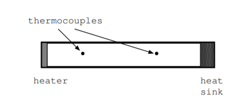
The apparatus to measure thermal conductivity consists of a heater, a heat sink, and a number of thermocouples [110] [112]. To measure thermal conductivity experimentally, start with a bar of material with a known cross sectional area \(A\). Heat one end of the bar with respect to the other, wait for a steady thermal state, and measure the temperature at each end of the bar. Next, calculate the temperature gradient \(\frac{dT}{dx}\) in units \(\text{K}{m}\) along the length of the bar. Also measure the rate that heat is supplied to the bar, \(\frac{d\mathbb{Q}}{dt}\), in units \(\frac{J}{s}\). By definition, thermal conductivity is the ratio
\[\kappa = \frac{\text{(power dissipated in heater)(distance between thermocouples)}}{\text{(cross sectional area)(change in temp)}} \nonumber \]
[109, p. 49]. The thermal conductivity can be calculated from
\[\kappa = \frac{- \left( \frac{d\mathbb{Q}}{dt} \right)}{A \left( \frac{dT}{dx} \right)}. \nonumber \]
This technique works well for low to moderate temperatures and materials with high thermal conductivity. Other methods exist to measure thermal conductivity and are advantageous for different temperature or conductivity ranges.
Another way to understand thermal conductivity is to think of it as the product of the amount of heat transported by some particle times the velocity of that particle. This viewpoint applies whether or not actual particles are involved in the heat transport. More specifically, thermal conductivity is given by
\[\kappa = C_v|\overrightarrow{v}|l \nonumber \]
The symbol \(C_v\) represents the specific heat at constant volume in \(\frac{J}{g \cdot K}\), and the symbol \(|\overrightarrow{v}|\)represents the magnitude of the transport velocity in \(\frac{m}{s}\). The scattering length is represented by \(l\) in \(m\).
Regardless of whether electrons, phonons, or something else transports heat through a material, the ability of that heat to get from one end to the other without being scattered or blocked influences the thermal conductivity. Thus, crystals typically have higher thermal conductivity than amorphous materials [113]. The thermal conductivity of a crystal can be lowered by exposing the material to radiation which destroys the crystallinity and increases the likelihood that the heat carrier will be scattered [110]. For glasses, scattering length is roughly the interatomic spacing [112]. Also, thermal conductivity of glasses is less temperature dependent than crystals because high temperatures distort the perfect crystallinity, thereby lowering the thermal conductivity for crystals but not glasses [113].
All the contributing factors, \(C_v\), \(|\overrightarrow{v}|\), and scattering length \(l\), are temperature dependent, so the thermal conductivity is a function of temperature. The temperature dependence of the factors is discussed in reference [110]. Thermal conductivity, like electrical conductivity, is low at low temperatures then rises to a maximum before decreasing again at higher temperatures [112].
Figure of Merit
The figure of merit of a thermoelectric device, \(Z\), is a single measure that summarizes how good a material is for making thermoelectric devices. It is defined as
\[Z = \frac{$^2 \sigma}{\kappa}, \nonumber \]
and it has units \(K^{-1}\). It depends on the Seebeck coefficient \($\), electrical conductivity \(\sigma\), and thermal conductivity \(\kappa\). A large value of \(Z\) indicates that the material is a good choice for use in construction of a thermoelectric device.
The figure of merit depends on temperature because the parameters \($\), \(\sigma\), and \(\kappa\) are strong functions of temperature. Thus, the best choice material for a thermoelectric device operating near room temperature may not be the best choice for a device operating at other temperatures. Sometimes \(ZT\) is used as a measure instead of just \(Z\) to account for the temperature dependence.
The figure of merit does not incorporate all of the temperature related factors to consider in selecting materials for thermoelectric devices. Melting temperature is also important. A thermoelectric device converts more energy when a larger temperature difference is placed across the device. The Seebeck coefficient is inversely proportional to the temperature differential, \($ = \frac{\Delta V}{\Delta T}\). However, too large of a temperature differential will melt the hot end of the device, and different materials can have very different melting temperatures. For example, lead telluride PbTe melts at \(924 ^{\circ}C\), and Bi\(_2\)Te\(_3\) melts at \(580 ^{\circ}C\) [114, p. 4-52, 4-71].
The figure of merit also depends on doping level because the electrical conductivity is directly proportional to the charge concentrations \(n\) and \(p\) [110]. Thus, a thermoelectric device made from a doped semiconductor has a higher electrical conductivity and thermoelectric efficiency than a device made from an undoped semiconductor of the same material. The Seebeck coefficient is also dependent on doping level but not as strongly [110]. Thermal conductivity is not a strong function of charge concentrations \(n\) and \(p\) [110]. Thus, thermoelectric materials are often made from heavily doped semiconductors or from conductors.
The figure of merit also depends on degree of crystallinity. Typically, both the electrical conductivity and thermal conductivity are much higher in crystals than glasses because charge and heat carriers are less likely to get scattered as they travel through crystals than glasses [113]. Since both electrical and thermal conductivity are influenced, the effect of degree of crystallinity on the figure of merit can be complicated.
Thermoelectric devices are typically made from junctions of two different metals or semiconductors. Essentially, a thermoelectric device is a diode. Common materials used include bismuth telluride, lead telluride, and antimony telluride, all of which are semimetals. Bi, Sb, and Pb are all located near each other on the periodic table. Other materials studied for use in thermoelectric devices include [110], BiSeTe, LiMnO, LiFeO, LiCoO, LiNiO, PbS, and ZnSb. These materials are either small gap semiconductors or semimetals. In semiconductor materials with small energy gaps, the ratio of electrical conductivity to thermal conductivity is large. However, this fact must be balanced against the fact that smaller gap semiconductors tend to have lower melting temperatures than larger gap semiconductors [110, ch. 1].
Recently, layered materials and superlattices have been considered as materials for thermoelectric devices [115] [116]. The layers can be tailored to affect the thermal and electrical properties differently and can act like a filter to select out different conduction mechanisms. Understanding of the conductivity mechanisms is a prerequisite to understanding such more complicated structures.