
8.3: Implementing a MUX
- Page ID
- 26997

\( \newcommand{\vecs}[1]{\overset { \scriptstyle \rightharpoonup} {\mathbf{#1}} } \)
\( \newcommand{\vecd}[1]{\overset{-\!-\!\rightharpoonup}{\vphantom{a}\smash {#1}}} \)
\( \newcommand{\id}{\mathrm{id}}\) \( \newcommand{\Span}{\mathrm{span}}\)
( \newcommand{\kernel}{\mathrm{null}\,}\) \( \newcommand{\range}{\mathrm{range}\,}\)
\( \newcommand{\RealPart}{\mathrm{Re}}\) \( \newcommand{\ImaginaryPart}{\mathrm{Im}}\)
\( \newcommand{\Argument}{\mathrm{Arg}}\) \( \newcommand{\norm}[1]{\| #1 \|}\)
\( \newcommand{\inner}[2]{\langle #1, #2 \rangle}\)
\( \newcommand{\Span}{\mathrm{span}}\)
\( \newcommand{\id}{\mathrm{id}}\)
\( \newcommand{\Span}{\mathrm{span}}\)
\( \newcommand{\kernel}{\mathrm{null}\,}\)
\( \newcommand{\range}{\mathrm{range}\,}\)
\( \newcommand{\RealPart}{\mathrm{Re}}\)
\( \newcommand{\ImaginaryPart}{\mathrm{Im}}\)
\( \newcommand{\Argument}{\mathrm{Arg}}\)
\( \newcommand{\norm}[1]{\| #1 \|}\)
\( \newcommand{\inner}[2]{\langle #1, #2 \rangle}\)
\( \newcommand{\Span}{\mathrm{span}}\) \( \newcommand{\AA}{\unicode[.8,0]{x212B}}\)
\( \newcommand{\vectorA}[1]{\vec{#1}} % arrow\)
\( \newcommand{\vectorAt}[1]{\vec{\text{#1}}} % arrow\)
\( \newcommand{\vectorB}[1]{\overset { \scriptstyle \rightharpoonup} {\mathbf{#1}} } \)
\( \newcommand{\vectorC}[1]{\textbf{#1}} \)
\( \newcommand{\vectorD}[1]{\overrightarrow{#1}} \)
\( \newcommand{\vectorDt}[1]{\overrightarrow{\text{#1}}} \)
\( \newcommand{\vectE}[1]{\overset{-\!-\!\rightharpoonup}{\vphantom{a}\smash{\mathbf {#1}}}} \)
\( \newcommand{\vecs}[1]{\overset { \scriptstyle \rightharpoonup} {\mathbf{#1}} } \)
\( \newcommand{\vecd}[1]{\overset{-\!-\!\rightharpoonup}{\vphantom{a}\smash {#1}}} \)
\(\newcommand{\avec}{\mathbf a}\) \(\newcommand{\bvec}{\mathbf b}\) \(\newcommand{\cvec}{\mathbf c}\) \(\newcommand{\dvec}{\mathbf d}\) \(\newcommand{\dtil}{\widetilde{\mathbf d}}\) \(\newcommand{\evec}{\mathbf e}\) \(\newcommand{\fvec}{\mathbf f}\) \(\newcommand{\nvec}{\mathbf n}\) \(\newcommand{\pvec}{\mathbf p}\) \(\newcommand{\qvec}{\mathbf q}\) \(\newcommand{\svec}{\mathbf s}\) \(\newcommand{\tvec}{\mathbf t}\) \(\newcommand{\uvec}{\mathbf u}\) \(\newcommand{\vvec}{\mathbf v}\) \(\newcommand{\wvec}{\mathbf w}\) \(\newcommand{\xvec}{\mathbf x}\) \(\newcommand{\yvec}{\mathbf y}\) \(\newcommand{\zvec}{\mathbf z}\) \(\newcommand{\rvec}{\mathbf r}\) \(\newcommand{\mvec}{\mathbf m}\) \(\newcommand{\zerovec}{\mathbf 0}\) \(\newcommand{\onevec}{\mathbf 1}\) \(\newcommand{\real}{\mathbb R}\) \(\newcommand{\twovec}[2]{\left[\begin{array}{r}#1 \\ #2 \end{array}\right]}\) \(\newcommand{\ctwovec}[2]{\left[\begin{array}{c}#1 \\ #2 \end{array}\right]}\) \(\newcommand{\threevec}[3]{\left[\begin{array}{r}#1 \\ #2 \\ #3 \end{array}\right]}\) \(\newcommand{\cthreevec}[3]{\left[\begin{array}{c}#1 \\ #2 \\ #3 \end{array}\right]}\) \(\newcommand{\fourvec}[4]{\left[\begin{array}{r}#1 \\ #2 \\ #3 \\ #4 \end{array}\right]}\) \(\newcommand{\cfourvec}[4]{\left[\begin{array}{c}#1 \\ #2 \\ #3 \\ #4 \end{array}\right]}\) \(\newcommand{\fivevec}[5]{\left[\begin{array}{r}#1 \\ #2 \\ #3 \\ #4 \\ #5 \\ \end{array}\right]}\) \(\newcommand{\cfivevec}[5]{\left[\begin{array}{c}#1 \\ #2 \\ #3 \\ #4 \\ #5 \\ \end{array}\right]}\) \(\newcommand{\mattwo}[4]{\left[\begin{array}{rr}#1 \amp #2 \\ #3 \amp #4 \\ \end{array}\right]}\) \(\newcommand{\laspan}[1]{\text{Span}\{#1\}}\) \(\newcommand{\bcal}{\cal B}\) \(\newcommand{\ccal}{\cal C}\) \(\newcommand{\scal}{\cal S}\) \(\newcommand{\wcal}{\cal W}\) \(\newcommand{\ecal}{\cal E}\) \(\newcommand{\coords}[2]{\left\{#1\right\}_{#2}}\) \(\newcommand{\gray}[1]{\color{gray}{#1}}\) \(\newcommand{\lgray}[1]{\color{lightgray}{#1}}\) \(\newcommand{\rank}{\operatorname{rank}}\) \(\newcommand{\row}{\text{Row}}\) \(\newcommand{\col}{\text{Col}}\) \(\renewcommand{\row}{\text{Row}}\) \(\newcommand{\nul}{\text{Nul}}\) \(\newcommand{\var}{\text{Var}}\) \(\newcommand{\corr}{\text{corr}}\) \(\newcommand{\len}[1]{\left|#1\right|}\) \(\newcommand{\bbar}{\overline{\bvec}}\) \(\newcommand{\bhat}{\widehat{\bvec}}\) \(\newcommand{\bperp}{\bvec^\perp}\) \(\newcommand{\xhat}{\widehat{\xvec}}\) \(\newcommand{\vhat}{\widehat{\vvec}}\) \(\newcommand{\uhat}{\widehat{\uvec}}\) \(\newcommand{\what}{\widehat{\wvec}}\) \(\newcommand{\Sighat}{\widehat{\Sigma}}\) \(\newcommand{\lt}{<}\) \(\newcommand{\gt}{>}\) \(\newcommand{\amp}{&}\) \(\definecolor{fillinmathshade}{gray}{0.9}\)Figure \(\PageIndex{1}\) shows how to implement a multiplexer circuit on a breadboard using only 7808 (AND), 7804 (OR) and 7832 (OR) chips. It begins by using the circuit which was implemented in Chapter 7.2.
The input values to the MUX are "1 0 1 0", as shown in Figure 8.2.2. These are hard coded values, and implemented in the circuits as direct connections to the positive and ground rails on the breadboard.
- Start with the decoder circuit which was implemented in Chapter 7.2.
- Install a 7408 (AND) chip to the board and power it.
- Install a 7432 (OR) chip to the board and power it.
- Wire the output from the A'B' gate in the decoder circuit (pin 11 on the 7408 chip labeled 1b) and wire it to the first input on the fourth AND gate (pin 13 on the 7408 labeled 2). Connect the second input to the AND gate (pin 12 on chip labeled 2) to a value of 1 by connecting it directly to the positive rail. The output of this AND gate (pin 11 on chip labeled 2) is forwarded to the 7432 (OR) chip.
- Wire the output from the A'B gate in the decoder circuit (pin 8 on the 7408 labeled 1b) and wire it to the third AND gate (pin 10 on the 7408 chip labeled 2). Connect the second input to the AND gate (pin 9 on chip labeled 2) to a value of 0 by connecting it directly to the ground rail. The output of this AND gate (pin 8 on chip labeled 2) is forwarded to the 7432 (OR) chip.
- Wire the output from the AB' gate in the decoder circuit (pin 3 on the 7408 chip labeled 1b) and wire it to the first AND gate (pin 1 on the 7408 labeled 2). Connect the second input to the AND gate (pin 2 on the chip labeled 2) to a value of 1 by connecting it directly to the positive rail. The output of this AND gate (pin 3 on chip labeled 2) is forwarded to the 7432 (OR) chip.
Figure \(\PageIndex{1}\): 4-to-1 MUX 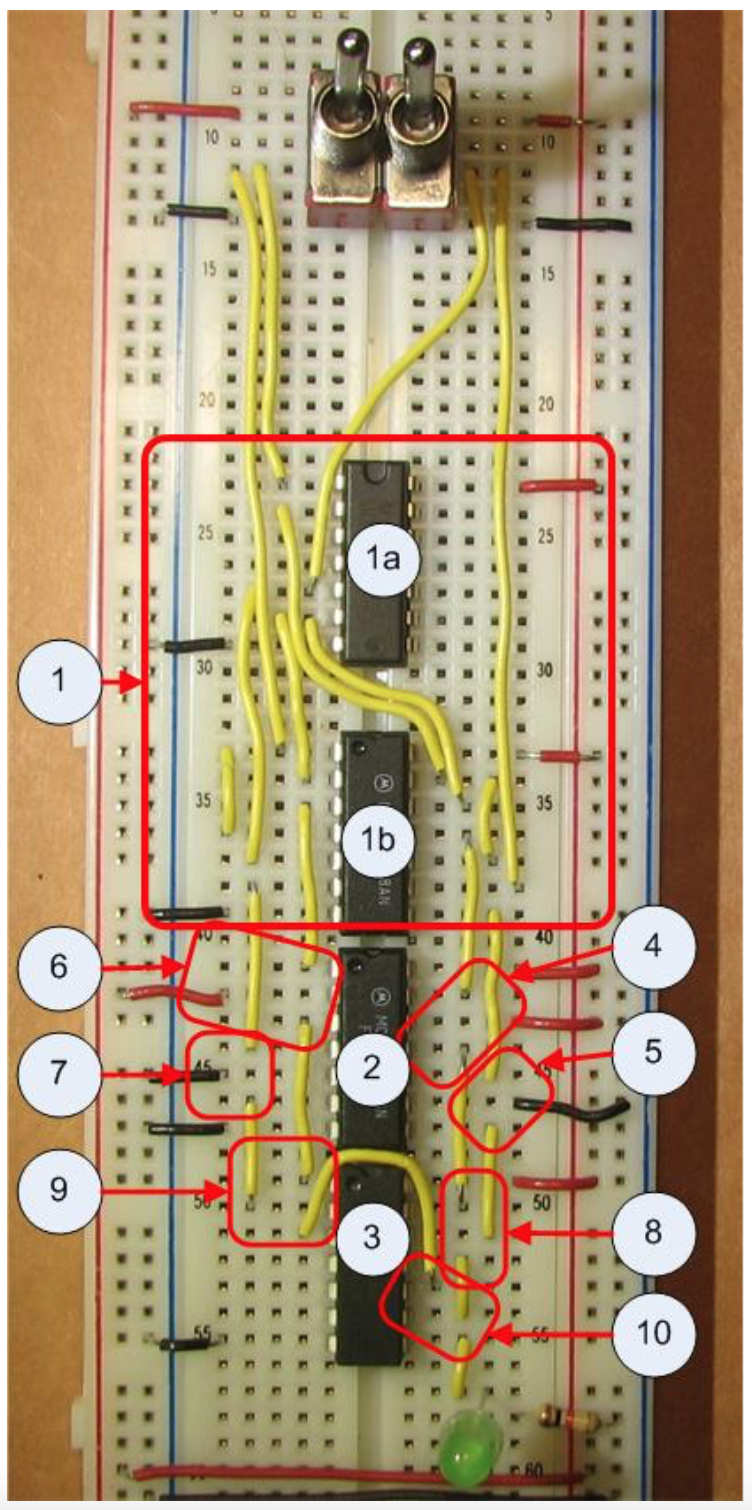
- Wire the output from the AB gate in the decoder circuit (pin 6 on the 7408 chip labeled 1b) and wire it to the second AND gate (pin 4 on the 7408 chip labeled 2). Connect the second input to the AND gate (pin 5 on chip labeled 2) to a value of 0 by connecting it directly to the ground rail. The output of this AND gate (pin 6 on chip labeled 2) is forwarded to the 7432 (OR) chip.
- Forward two of the input values from the AND gate (pins 11 and 8 on the 7408 chip) by sending them to the fourth OR gate (pins 12 and 13 on the 7482 chip).
- Forward two of the input values from the AND gate (pins 3 and 6 on the 7408 chip) by sending them to the first OR gate (pins 1 and 2 on the 7482 chip).
- Forward the final output for the MUX by connecting the output of the first and fourth OR gate (pins 3 and 11 on the 7432 chip) to the input of the third OR gate (pins 9 and 10 on the 7432 chip). The output of the circuit is from the third OR gate (pin 8 of the 7432 chip). It is sent to the LED as the output from the MUX.
The MUX should now light when the switches A and B are in positions A'B' and AB'. The implementation of the MUX can be further tested by changing the input to the MUX by switching the inputs to the MUX, e.g. changing the rail to which pins 2, 5, 9, and 12 are connected.