
5.2: Frequency-Dependent Characteristics
- Page ID
- 41284

In this section the origins of the frequency-dependent behavior of a microstrip line are examined. The most important frequency-dependent
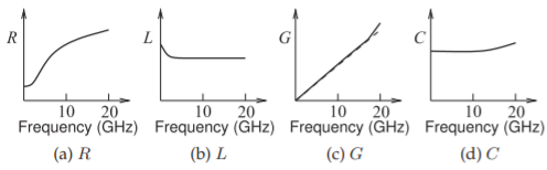
Figure \(\PageIndex{1}\) Frequency dependence of transmission line parameters.
effects are
- changes of material properties (permittivity, permeability, and conductivity) with frequency (Section 5.2.1),
- current bunching (discussed in Section 5.2.3),
- skin effect (Sections 5.2.4 and 5.2.5),
- internal conductor inductance variation (Section 5.2.4),
- dielectric dispersion (Section 5.2.6), and
- multimoding (Section 5.3).
5.2.1 Material Dependency
Changes of permittivity, permeability, and conductivity with frequency are properties of the materials used. Fortunately the characteristics microwave materials are almost independent of frequency, at least up to \(300\text{ GHz}\).
5.2.2 Frequency-Dependent Charge Distribution
Skin effect, current bunching, and internal conductor inductance are all due to the necessary delay in transferring EM information from one location to another. This information cannot travel faster than the speed of light in the medium. In a dielectric material the speed of an EM wave will be slower than that in free space by a factor of \(\sqrt{\varepsilon_{r}}\), e.g. \(c/3.2\) for \(\varepsilon_{r} = 10\). The velocity in a conductor is extremely low, around \(c/1000\), because of high conductivity. In brief, current bunching is due to changes related to the finite velocity of information transfer through the dielectric, and skin effect is due to the very slow speed of information transfer inside a conductor. As frequency increases, only limited information to rearrange charges can be sent before the polarity of the signal reverses and information is ‘sent’ to reverse the changes. The skin and charge-bunching effects on a microstrip line are illustrated in Figure \(\PageIndex{3}\).
5.2.3 Current Bunching
Consider the microstrip charge distribution shown in Figure \(\PageIndex{3}\). The thickness of the microstrip is often a significant fraction of its width, although this is exaggerated here.
The charge distribution shown in Figure \(\PageIndex{3}\)(a) applies when there is a positive DC voltage on the strip and the positive charges on the top conductor arranged with a fairly uniform distribution. The individual positive charges tend to repel each other, but this has little effect on the
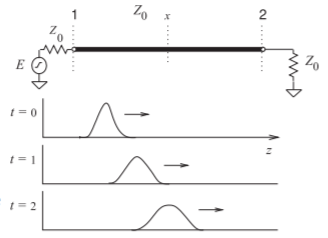
Figure \(\PageIndex{2}\): Dispersion of a pulse along a line.
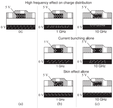
Figure \(\PageIndex{3}\): Cross-sectional view of the charge distribution on an interconnect at different frequencies. The \(+\) and \(−\) indicate charge concentrations of different polarity and corresponding current densities. There is no current bunching or skin effect at DC.
charge distribution at low frequencies for practical conductors with finite conductivity. On the ground plane there are balancing negative charges which are uniformly distributed across the whole of the ground plane. The charge distribution at DC, indicates that current would flow uniformly throughout the strip and the return current in the ground plane would be distributed over the whole of the ground plane.
The charge distribution becomes less uniform as frequency increases and eventually the signal changes so quickly that information to rearrange charges on the ground plane is soon (half a period latter) countered by reverse instructions. Thus the charge distribution depends on how fast the signaling changes. One way of looking at this effect is to view the charges on the strip of the microstrip line at one time. This is shown in Figure \(\PageIndex{4}\) for a DC signal on the line and for a high-frequency signal.
The electric field lines, which must originate and terminate on charges, will concentrate in the substrate more closely under the strip as frequency increases. The two major effects are that the effective permittivity of the microstrip line increases with frequency, and resistive loss increases as the current density in the ground, which corresponds to the net charge density, increases. Thus the line resistance and capacitance increase with frequency, see Figures \(\PageIndex{1}\)(a and d). For the majority of substrates \(G\) is due to dielectric relaxation and so increases linearly with frequency with a superlinear increase at very high frequencies when the electric field is more concentrated in the dielectric, see Figure \(\PageIndex{1}\)(c).
In the frequency domain the current bunching effects are seen in the higher-frequency views shown in Figures \(\PageIndex{3}\)(b and c). (The concentration of charges near the metal surface is a separate effect known as the skin effect.)
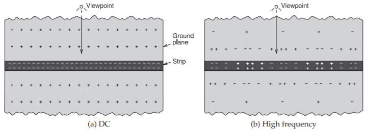
Figure \(PageIndex{4}\): Current bunching effect in time. Positive and negative charges are shown on the strip and on the ground plane. The viewpoint is on the ground plane.
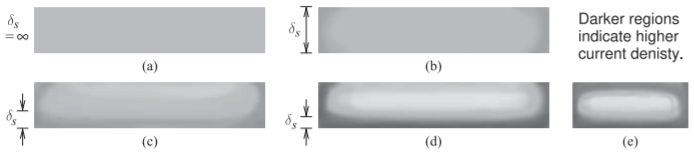
Figure \(\PageIndex{5}\): Cross-sections of the strip of a microstrip line showing the impact of skin effect and current bunching on current density: (a) at dc (uniform current density); (b) the strip thickness, \(t\), is equal to the skin depth, \(\delta_{s}\) (i.e. at a low microwave frequency); (c) \(t = 3\delta_{s}\); (d) \(t = 5\delta_{s}\) (i.e. at a high microwave frequency); and (e) \(t = 5\delta_{s}\) for a narrow strip. The plots are the result of 3D simulations of a microstrip line using internal conductor gridding.
5.2.4 Skin Effect and Internal Conductor Inductance
At low frequencies, currents are distributed uniformly throughout a conductor. Thus there are magnetic fields inside the conductor and hence magnetic energy storage. As a result, there is additional inductance. Transferring charge to the interior of conductors is particularly slow, and as the frequency of the signal increases, charges are confined closer to the surface of the metal, see Figure \(\PageIndex{5}\). This phenomenon is known as the skin effect. With lower internal currents, the internal conductor inductance reduces and the total inductance of the line drops, see Figure \(\PageIndex{1}\)(b). Only above a few gigahertz or so can the line inductance be approximated as being constant for a typical microstrip line.
The skin depth, \(\delta_{s}\), is the distance at which the electric field, or the charge density, reduces to \(1/e\) of its value at the surface. The skin depth is
\[\label{eq:1}\delta_{s}=1/\sqrt{\pi f\mu_{0}\sigma_{2}} \]
Here \(f\) is frequency and \(\sigma_{2}\) is the conductivity of the conductor. The (real part of the) permittivity and permeability of metals typically used for interconnects (e.g., gold, silver, copper, and aluminum) are that of free space as there is no mechanism to store additional electric or magnetic energy.
5.2.5 Skin Effect and Line Resistance
The skin effect is illustrated in Figure \(\PageIndex{3}\)(b) at \(1\text{ GHz}\). The situation is more extreme as the frequency continues to increase. There are several important consequences of this. On the top conductor, as frequency increases, current flow is mostly concentrated near the surface of the conductors and the effective cross-sectional area of the conductor, as far as the current is concerned, is less. Thus the resistance of the top conductor increases. A more dramatic situation exists for the charge in the ground plane which becomes more concentrated under the strip. In addition to this, charges and current are confined to the skin of the ground conductor so that the frequency-dependent relative change of ground plane resistance with increasing frequency is greater than that of the strip.
The skin effect and current bunching result in frequency dependence of the line resistance, \(R\), with
\[\label{eq:2}R(f)=\left\{\begin{array}{ll}{R(0)}&{f\text{ such that }t\leq 3\delta_{s}}\\ {R(0)+R_{\text{skin}}(f)}&{f\text{ such that }t> 3\delta_{s}} \end{array} \right. \]
where \(R(0) = R_{\text{strip}}(0) + R_{\text{ground}}(0)\) is the resistance of the line at low frequencies. \(R(f)\) describes the frequency-dependent line resistance that is due to both the skin effect and current bunching. Approximately
\[\label{eq:3}R_{\text{skin}}(f)=R(0)k\sqrt{f} \]
where \(k\) is a geometry-dependent constant. Note that it is pointless to make a strip or of ground thicker than three times the skin depth.
Example \(\PageIndex{1}\): Skin Depth
Determine the skin depth for copper (Cu), silver (Ag), aluminum (Al), gold (Au), and titanium (Ti) at \(100\text{ MHz},\: 1\text{ GHz},\: 10\text{ GHz}\), and \(100\text{ GHz}\).
Solution
The skin depth is calculated using Equation \(\eqref{eq:1}\).
| Metal |
Resistivity \((n\Omega\cdot\text{m})\) | Conductivity \((\text{MS/m})\) | Skin depth, \(\delta_{s}\text{ (}\mu\text{m)}\) | |||
|---|---|---|---|---|---|---|
| \(100\text{ MHz}\) | \(1\text{ GHz}\) | \(10\text{ GHz}\) | \(100\text{ GHz}\) | |||
| Copper (Cu) | \(16.78\) | \(59.60\) | \(6.52\) | \(2.06\) | \(0.652\) | \(0.206\) |
| Silver (Ag) | \(15.87\) | \(63.01\) | \(6.34\) | \(2.01\) | \(0.634\) | \(0.201\) |
| Aluminum (Al) | \(26.50\) | \(37.74\) | \(8.19\) | \(2.59\) | \(0.819\) | \(0.259\) |
| Gold (Ag) | \(22.14\) | \(45.17\) | \(7.489\) | \(2.37\) | \(0.749\) | \(0.237\) |
| Titanium (Ti) | \(4200\) | \(0.2381\) | \(103.1\) | \(32.6\) | \(10.3\) | \(3.26\) |
Table \(\PageIndex{1}\)
5.2.6 Dielectric Dispersion
Dispersion is principally the result of the propagation velocity of a sinusoidal signal being dependent on frequency since the effective permittivity is frequency-dependent. The electric field lines shift as a result with more of the electric energy being in the dielectric as frequency increases. At high frequencies the rearrangement results in the capacitance of the line increases—typically less than \(10\%\) from DC to \(100\text{ GHz}\).
The limits of \(\varepsilon_{e}(f)\) are readily established; at the low-frequency extreme it reduces to the static TEM value \(\varepsilon_{e}\) (or \(\varepsilon_{e}(0)\)), while as frequency is increased indefinitely, \(\varepsilon_{e}(f)\) approaches the substrate permittivity itself, \(\varepsilon_{r}\). That is,
\[\label{eq:4}\varepsilon_{e}(f)\to\left\{\begin{array}{ll}{\varepsilon_{e}(0)}&{\text{as }f\to 0}\\{\varepsilon_{r}}&{\text{as }f\to ∞}\end{array}\right. \]
where \(\varepsilon_{e}(0)\) is given by Equation (4.4.12). Detailed analysis yields
\[\label{eq:5}\varepsilon_{e}(f)=\varepsilon_{r}-\frac{\varepsilon_{r}-\varepsilon_{e}(0)}{1+(f/f_{a})^{m}} \]
where \(m\) and \(f_{a}\) depend on \(w,\: h,\) and \(\varepsilon_{r}\), see Section 24.3 of [1]. Very approximately \(m ≈ 2\) and \(f_{a} ≈ 50\text{ GHz}\) for a \(50\:\Omega\) microstrip line with/ a \(500\:\mu\text{m}\) substrate. The frequency-dependent characteristic impedance is
\[\label{eq:6}Z_{0}(f)=Z_{0}(0)\frac{\sqrt{\varepsilon_{e}(0)}}{\varepsilon_{e}(f)} \]
where \(Z_{0}(0)\) is the low-frequency value given by Equation (4.4.9).
5.2.7 Summary
For microstrip, with increasing frequency the proportion of signal energy in the air region reduces and the proportion in the dielectric increases. The overall trend is for the fields to be more concentrated in the dielectric as frequency increases and thus effective relative permittivity increases.