
10.10: Impedance Matching Using Smith Charts
- Page ID
- 41332

The lumped-element matching networks presented up to now can also be developed using Smith charts which provide a fairly intuitive approach to network design. With experience it will be found that this is the preferred approach to developing designs, as trade-offs can be captured graphically. Smith chart-based design will be presented using examples.
10.7.1 Two-Element Matching
The examples here build on the preceding lumped-element matching network design and now use the Smith. Capacitive and inductive regions on the Smith chart are shown in Figure \(\PageIndex{1}\). In the design examples presented here, circles of constant resistance or constant conductance are followed and these correspond to varying reactance or susceptance, respectively.
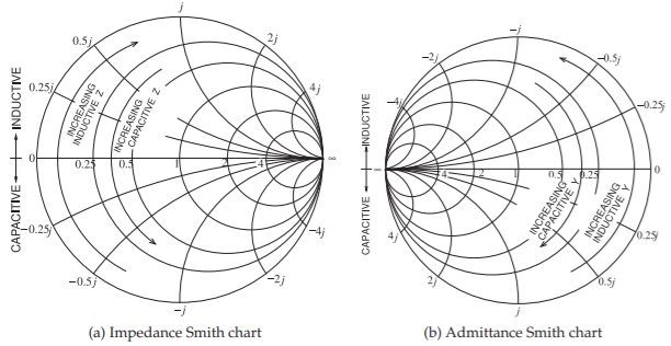
Figure \(\PageIndex{1}\): Inductive and capacitive regions on Smith charts. Increasing capacitive impedance (\(Z\)) indicates smaller capacitance; increasing inductive admittance (\(Y\)) indicates smaller inductance.
Example \(\PageIndex{1}\): Two-Element Matching Network Design Using a Smith Chart
Develop a two-element matching network to match a source with an impedance of \(R_{S} = 25\:\Omega\) to a load \(R_{L} = 200\:\Omega\) (see Figure \(\PageIndex{2}\)).
Solution
The design objective is to present conjugate matched impedances to the source and load. However, since here the source and load impedances are real, the design objective is \(Z_{1} = R_{S}\) and \(Z_{2} = R_{L}\). The load and source resistances are plotted on the Smith chart in Figure \(\PageIndex{4}\)(a) after choosing a normalization impedance of \(Z_{0} = 50\:\Omega\) (and so \(r_{S} = R_{S}/Z_{0} = 0.5\) and \(r_{L}= R_{L}/Z_{0} = \)4). The normalized source impedance, \(r_{S}\), is Point \(\mathsf{A}\), and the normalized load impedance, \(r_{L}\), is Point \(\mathsf{C}\). The matching network must be lossless, which means that the design must follow lines of constant resistance (on the impedance part of the Smith chart) or constant conductance (on the admittance part of the Smith chart). So Points \(\mathsf{A}\) and \(\mathsf{C}\) must be on the above circles and the circles must intersect if a design is possible. The design can be viewed as moving back from the source toward the load or moving back from the load toward the source. (The views result in identical designs.) Here the view taken is moving back from the source toward the load.
One possible design is shown in Figure \(\PageIndex{4}\)(a). From Point \(\mathsf{A}\), the line of constant resistance is followed to Point \(\mathsf{B}\) (there is increasing series reactance along this path). From Point \(\mathsf{B}\), the locus follows a line of constant conductance to the final point, Point \(\mathsf{C}\). There is also an alternative design that follows the path shown in Figure \(\PageIndex{4}\)(b). There are only two designs that have a path from \(\mathsf{A}\) to \(\mathsf{B}\) following just two arcs. At this point two designs have been outlined. The next step is assigning element values.
The design shown in Figure \(\PageIndex{4}\)(a) begins with \(r_{S}\) followed by a series reactance, \(x_{S}\), taking the locus from \(\mathsf{A}\) to \(\mathsf{B}\). Then a shunt capacitive susceptance, \(b_{P}\), takes the locus from \(\mathsf{B}\) to \(\mathsf{C}\) and \(r_{L}\). At Point \(\mathsf{A}\) the reactance \(x_{A} = 0\), at Point \(\mathsf{B}\) the reactance \(x_{B} = 1.323\). This value is read off the Smith chart, requiring that an arc as shown be interpolated between the arcs provided. It should be noted that not all versions of Smith charts include negative signs, as the chart becomes too complicated. Thus the user needs to be aware and add signs where appropriate. The normalized series reactance is
\[\label{eq:1} x_{S}=x_{B}-x_{A}=1.323-0=1.323 \]
that is,
\[\label{eq:2} X_{S}=x_{s}Z_{0}=1.323\times 50=66.1\:\Omega \]
A shunt capacitive element takes the locus from Point \(\mathsf{B}\) to Point \(\mathsf{C}\) and
\[\label{eq:3}b_{P}=b_{C}-b_{B}=0-(-0.661)=0.661 \]
so
\[\label{eq:4}B_{P}=b_{P}/Z_{0}=0.661/50=13.22\text{ mS}\quad\text{or}\quad X_{P}=-1/B_{P}=-75.6\:\Omega \]
The final design is shown in Figure \(\PageIndex{3}\).
One of the advantages of using the Smith chart is that the design progresses in stages, with the structure of the design developed before actual numerical values are calculated. Of course, it is difficult to extract accurate values from a chart, so designs are regularly roughed out on a Smith chart and refined using CAD tools. Example \(\PageIndex{1}\) matched a resistive source to a resistive load. The next example considers the matching of complex load
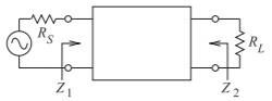
Figure \(\PageIndex{2}\): Design objectives for Example \(\PageIndex{1}\). \(R_{S} = 15\:\Omega ,\: R_{L} = 200\:\Omega\).
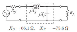
Figure \(\PageIndex{3}\): Final design for Example \(\PageIndex{1}\) using the path shown in Figure \(\PageIndex{4}\)(a).
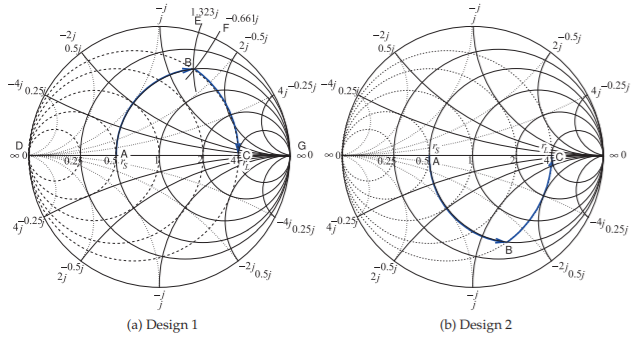
Figure \(\PageIndex{4}\): Alternative designs for Example \(\PageIndex{1}\). The normalization impedance is \(50\:\Omega\).
and source impedances. In the earlier algorithmic approach to matching network design absorption and resonance were introduced as strategies for dealing with complex terminations. Design was not always straightforward. This complication disappears with a Smith chart-based design, as it is conceptually not much different from the resistive problem of Example \(\PageIndex{1}\).
Example \(\PageIndex{2}\): Matching Network Design With Complex Impedances
Develop a two-element matching network to match a source with an impedance of \(Z_{S} = 12.5 + 12.5\jmath\:\Omega\) to a load \(Z_{L} = 50 − 50\jmath\:\Omega\), as shown in Figure \(\PageIndex{5}\).
Solution
The design objective is to present conjugate matched impedances to the source and load; that is, \(Z_{1} = Z_{S}^{\ast}\)S and \(Z_{2} = Z_{L}^{\ast}\). The choice here is to design for \(Z_{1}\); that is, elements will be inserted in front of \(Z_{L}\) to produce the impedance \(Z_{1}\). The normalized source and load impedances are plotted in Figure \(\PageIndex{6}\)(a) using a normalization impedance of \(Z_{0} = 50\:\Omega\), so \(z_{S} = Z_{S}/Z_{0} = 0.25 + 0.25\jmath\) (Point \(\mathsf{S}\)) and \(z_{L} = Z_{L}/Z_{0} = 1 −\jmath\) (Point \(\mathsf{C}\)).
The impedance to be synthesized is \(z_{1} = Z_{1}/Z_{0} = z_{S}^{\ast} = 0.25− 0.25\jmath\) (Point \(\mathsf{A}\)). The matching network must be lossless, which means that the lumped-element design must follow lines of constant resistance (on the impedance part of the Smith chart) or constant conductance (on the admittance part of the Smith chart). Points \(\mathsf{A}\) and \(\mathsf{C}\) must be on the above circles and the circles must intersect if a design is possible.
The design can be viewed as moving back from the load impedance toward the conjugate of the source impedance. The direction of the impedance locus is important. One possible design is shown in Figure \(\PageIndex{6}\)(a). From Point \(\mathsf{C}\) the line of constant conductance is followed to Point \(\mathsf{B}\) (there is increasing positive [i.e., capacitive] shunt susceptance along this path). From Point \(\mathsf{B}\) the locus follows a line of constant resistance to the final point, Point \(\mathsf{A}\).
The design shown in Figure \(\PageIndex{6}\)(a) begins with a shunt susceptance, \(b_{P}\), taking the locus from Point \(\mathsf{C}\) to Point \(\mathsf{B}\) and then a series inductive reactance, \(x_{S}\), taking the locus to Point \(\mathsf{A}\). At Point \(\mathsf{C}\) the susceptance \(b_{C} = 0.5\), at Point \(\mathsf{B}\) the susceptance \(b_{B} = 1.323\). This value is read off the Smith chart, requiring that an arc of constant susceptance, as shown, be interpolated between the constant susceptance arcs provided. The normalized shunt susceptance is
\[\label{eq:5}b_{P}=b_{B}-b_{C}=1.323-05=0.823 \]
that is,
\[\label{eq:6}B_{P}=b_{P}/Z_{0}=0.823/(50\:\Omega )=16.5\text{ mS or }X_{P}=-1/B_{P}=-60.8\:\Omega \]
A series reactive element takes the locus from Point \(\mathsf{B}\) to Point \(\mathsf{A}\), so
\[\label{eq:7}x_{S}=x_{A}-x_{B}=-0.25-(-0.661)=0.411 \]
so
\[\label{eq:8}X_{S}=x_{S}Z_{0}=0.411\times 50\:\Omega =20.6\:\Omega \]
The final design is shown in Figure \(\PageIndex{7}\).
There are only two designs that have a path from Point \(\mathsf{C}\) to Point \(\mathsf{A}\) following just two arcs. In Design 1, shown in Figure \(\PageIndex{6}\)(a), Path \(\mathsf{CBA}\) is much shorter than Path \(\mathsf{CHA}\) for Design 2 shown in Figure \(\PageIndex{6}\)(b). The path length is an approximate indication of the total reactance required, and the higher the reactance, the greater the energy storage and hence the narrower the bandwidth of the design. (The actual relative bandwidth depends on the voltage and current levels in the network; the path length criteria, however, is an important rule of thumb.) Thus Design 1 can be expected to have a much
higher bandwidth than Design 2. Since designing broader bandwidth is usually an objective, a design requiring a shorter path on a Smith chart is usually preferable.
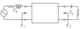
Figure \(\PageIndex{5}\): Design objectives for Example \(\PageIndex{2}\).
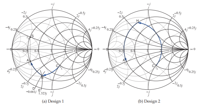
Figure \(\PageIndex{6}\): Smith chart-based designs used in Example \(\PageIndex{2}\). (\(50\:\Omega\) normalization used.)
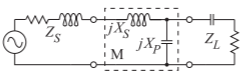
Figure \(\PageIndex{7}\): Final circuit for Design 1 of Example \(\PageIndex{2}\). \(X_{S} = 20.6\:\Omega ,\: X_{P} = −60.8\:\Omega\).