
25.2: ATmega ADC system
- Page ID
- 35903

A block diagram of the ATmega ADC system is found in Figure \(\PageIndex{1}\).
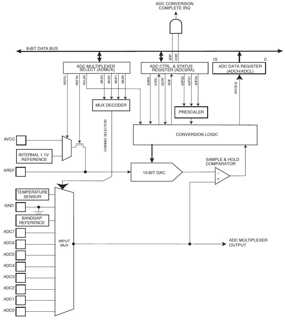
The heart of the system is a single successive approximation DAC with 10 bit resolution. Maximum conversion speed at full resolution is about 15 k samples per second. Clearly this is insufficient for applications such as CD quality audio or video but is more than fast enough for most sensor and user interface monitoring. The converter performance specifications include 0.5 LSB integral non-linearity error and ±2 LSB absolute accuracy. An on-board reference is available although an external reference may also be used. The converter includes a sample-and-hold system to stabilize the measurement for rapidly changing input signals. There is an eight channel mux although only six of these channels are used on some packages (the package used on the standard configuration of the Arduino Uno board uses six). The input circuitry is optimized for sources that have an output impedance of 10 KΩ or less. It is also very important to recognize that the system is unipolar and will only respond to positive voltages. If the signal to be measured is bipolar, some manner of DC level shifting will be required.
There are several registers associated with the ADC system. These are shown in Table \(\PageIndex{1}\).
| Register | Bit 7 | Bit 6 | Bit 5 | Bit 4 | Bit 3 | Bit 2 | Bit 1 | Bit 0 |
|---|---|---|---|---|---|---|---|---|
ADCSRA |
ADEN |
ADSC |
ADATE |
ADIF |
ADIE |
ADPS2 |
ADPS1 |
ADPS0 |
ADCSRB |
- | ACME |
- | - | - | ADTS2 |
ADTS1 |
ADTS0 |
ADMUX |
REFS1 |
REFS0 |
ADLAR |
- | MUX3 |
MUX2 |
MUX1 |
MUX0 |
ADCH |
ADC9/- |
ADC8/- |
ADC7/- |
ADC6/- |
ADC5/- |
ADC4/- |
ADC3/9 |
ADC2/8 |
ADCL |
ADC1/7 |
ADC0/6 |
-/ADC5 |
-/ADC4 |
-/ADC3 |
-/ADC2 |
-/ADC1 |
-/ADC0 |
ADCSRA and ADCSRB are the Analog-Digital Control and Status Registers. Here are their bit descriptions:
ADEN: ENable. Set to one to enable to Analog-Digital system.ADSC: Start Conversion. Set to one to start a conversion. When the conversion is complete, the hardware will reset this bit to zero. Writing zero to this bit will have no effect.ADATE: Auto Trigger Enable. Set to one for auto trigger mode. A rising edge on the selected trigger signal will start a conversion. The trigger source is selected via theADTSbits in theADCSRBregister (below).ADIF: Interrupt Flag. This is used with interrupt mode. This bit is set when a conversion is complete and the data registers are updated. This bit is cleared by the hardware when executing the interrupt handler routine. Use withADIE.ADIE: Interrupt Enabled. Set to one to enable the ADC conversion interrupt. Use withADIF.ADPS2-0: Prescaler bits. These bits are used to divide down the system clock to the ADC clock. 000 and 001 yield division by two and increasing values double the clock divide with 111 yielding divide by 128.ACME: Analog Comparator Multiplexer Enabled. Setting these bits allows any of the eight multiplexed ADC pins to replace the negative input to the analog comparator.ADTS2-0: Trigger Source. IfADATEis set to one, these bits determine the trigger source. 000 is free running mode, 001 triggers from the analog comparator, 010 uses External Interrupt Request 0, and the remaining values set various timer/counter sources.
ADMUX is the Analog-Digital MUltipleXer selection register. It is also used for reference selection and data justification. The bit descriptions follow:
REFS1-0: REFerence voltages. 00 yields theAREFpin, 01 yieldsAVCC, 11 yields internal 1.1 volt reference and 10 is reserved.ADLAR: Left Adjust Result. Setting this bit will left justify the output bits in theADCH/ADCLregisters. Setting to zero right justifies.MUX3-0: MUltipleXer. These bits select the input pin. 000 selectsADC0, 001 selectsADC1and so on to 1000 selectingADC8(the temperature sensor). 1110 selects the 1.1 volt reference and 1111 selects ground. All other values are reserved.
Finally we have ADCH and ADCL, the ADC High and Low output registers. There are two registers because this is a 10 bit converter but the registers only hold eight bits each. There are two modes of operation in conjunction with the ADLAR bit in the ADMUX register. If ADLAR is set then the top eight bits will be placed into ADCH and the bottom two bits will be placed at the top of ADCL. If ADLAR is cleared then the bottom eight bits will be found in ADCL and the top two bits will be found at the bottom of ADCH. Just think of the two registers as a single 16 bit register with the bits pushed to the left or right as shown in Table \(\PageIndex{2}\).
| ADCH | ADCL | |||||||||||||||
|---|---|---|---|---|---|---|---|---|---|---|---|---|---|---|---|---|
| ADLAR | Bit 15 | Bit 14 | Bit 13 | Bit 12 | Bit 11 | Bit 10 | Bit 9 | Bit 8 | Bit 7 | Bit 6 | Bit 5 | Bit 4 | Bit 3 | Bit 2 | Bit 1 | Bit 0 |
| 1 | ADC 9 | ADC 8 | ADC 7 | ADC 6 | ADC 5 | ADC 4 | ADC 3 | ADC 2 | ADC 1 | ADC 0 | - | - | - | - | - | - |
| 0 | - | - | - | - | - | - | ADC 9 | ADC 8 | ADC 7 | ADC 6 | ADC 5 | ADC 4 | ADC 3 | ADC 2 | ADC 1 | ADC 0 |
If only eight bits of resolution are needed, it is possible to left justify and read just ADCH, ignoring ADCL.
Single conversion operation is fairly straightforward. First, set up your initialization section. This begins with setting ADEN to enable the system. Then decide on the proper prescale value. The chip specifications indicate that the successive approximation circuitry will perform best with an ADC clock in the range of 50 kHz to 200 kHz. A typical conversion will take 13 ADC clock cycles (the first conversion will take 25 due to initialization overhead). Once this is determined, set ADLAR for data justification and REFS for the reference voltage. Then set the ADMUX bits to determine the input channel. Finally, set ADSC to start a conversion. You can wait on this bit or come back to it later. When the conversion is complete the hardware will reset it to zero. At that point read the value from ADCL and combine (shift and OR) with the value read from ADCH into a 16 bit integer. Note that you must read ADCL before reading ADCH. Reading ADCL locks the ADC registers preventing the hardware from overwriting the registers on a subsequent conversion. Reading ADCH unlocks them.
We will take a closer look at the software process in the next chapter.