
4.5: The Spatial Profile of the Potential
- Page ID
- 50033

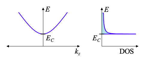
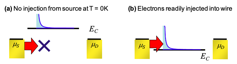
As shown in Figure \(\PageIndex{1}\), below, the wire may be described by its dispersion relation or by its density of states (DOS). The dispersion relation describes a band of conducting states. The bottom of the band is known as the conduction band edge. It corresponds to the lowest energy for a plane wave state in the wire. The conduction band edge is particularly important because its position controls the current flow in the wire. If it is below the source work function then electrons are readily injected into the wire. In contrast, if the conduction band edge is above the source workfunction, then current flow requires electrons with additional thermal energy.
The application of a bias may later the position of the conduction band edge by changing the local electrostatic potential, U. Two examples are shown in Figure 4.5.3, below.
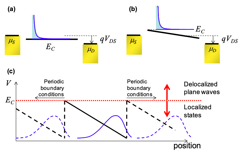
The first example in Figure 4.5.3 demonstrates a metallic wire under bias. In this limit there is no potential variation along the wire. In (b) of Figure 4.5.3 we present a wire with varying potential along its length. The conduction band edge, \(E_{C}\), occurs at the point of maximum repulsive potential. This is explained in (c) of Figure 4.5.3. Electronic wavefunctions in the wire with energies below \(E_{C}\) are localized and may only be accessed from the source by tunneling through a repulsive potential. Due to the relatively low rate of injection into these states we will ignore current through these modes in this class. Above \(E_{C}\), however, the electron wavefunctions are delocalized plane waves which readily transport electrons between the contacts.
Determining the potential profile of the wire can be Consider a point, z, on the wire. The electrostatic potential at point z is given by
\[ U(z) = -qV_{DS} \frac{C_{D}(z)}{C_{ES}(z)} \nonumber \]
where \(C_{D}\) is the capacitance linking the point at z to the drain, and \(C_{S}\) is the capacitance linking the point at z to the source, and \(C_{ES}(z)\) is the total electrostatic capacitance at z; \(C_{ES}(z)=C_{S}(z)+C_{D}(z)\).
If we assume that source and drain capacitances can be modeled by parallel plate capacitors, we found in Equation (3.5.5) that the potential varies linearly between the contacts. However, charging of the conductor can change the potential profile by opposing changes induced by the drain source voltage. Adding the effect of charging to Equation (4.5.1) gives:
\[ U = -qV_{DS}\frac{C_{D}}{C_{ES}}+\frac{q^{2}(N-N_{0})}{C_{ES}} \nonumber \]
Remember that all these electrostatic capacitances vary with position along the wire. Next, let's assume that applied bias is small and consequently the change in charge is small i.e. \(\delta N = N-N_{0}\). We can relate \(\delta N\) to the density of states at the Fermi level in the wire, \(g(E_{F})\), and the change in potential, \(\delta U\).
\[ \delta U = -q\delta V_{DS}\frac{C_{D}}{C_{ES}}-\frac{q^{2}g(E_{F})}{C_{ES}}\delta U \nonumber \]
Substituting the quantum capacitance \(C_{Q} = q^{2}g(E_{F})\) and collecting terms gives
\[ \delta U=-q\delta V_{DS} \frac{C_{D}}{C_{ES}+C_{Q}} \nonumber \]
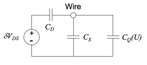
The equivalent circuit is shown in Figure 4.5.4. Note that the quantum capacitance depends on the position of the Fermi level within the DOS. Because the potential shifts the DOS relative to the Fermi level, the quantum capacitance also depends on the potential.
In this class we'll consider two extreme cases: \(C_{Q}\ggC_{ES}\) and \(C_{Q}\llC_{ES}\). The former case corresponds to a perfectly metallic wire. The later case can correspond to either a perfect insulator or a nanoscale conductor, which due to its size, has very few electronic states.
Perfectly metallic wires
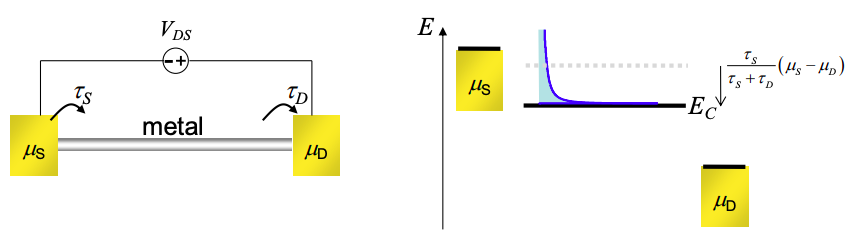
In the limit that \(C_{Q}\ggC_{ES}\), Equation (4.5.4) reduces to \(\delta U = 0\), meaning that the potential is fixed along the length of the wire by the large density of states at the Fermi Level. The potential of the wire relative to the contacts is then determined by the contact properties, in particular the coupling coefficients \(\tau_{S}\) and \(\tau_{D}\). The potential is determined from the analysis of Figure 3.9.1.
The Insulator/Nanoscale Limit
The spacing between k states in a 1-d conductor is simply \(\Delta k = 2\pi/L\), where L is the length of the wire. When L is small there are few states available for electrons. Consequently, insulators and many very small conductors have relatively few states for electrons at the Fermi level. We can ignore charging effects in these conductors. The potential is then simply described by Equation (4.5.1).