
5.13: Ballistic Quantum Well FETs
- Page ID
- 51624
\( \newcommand{\vecs}[1]{\overset { \scriptstyle \rightharpoonup} {\mathbf{#1}} } \)
\( \newcommand{\vecd}[1]{\overset{-\!-\!\rightharpoonup}{\vphantom{a}\smash {#1}}} \)
\( \newcommand{\dsum}{\displaystyle\sum\limits} \)
\( \newcommand{\dint}{\displaystyle\int\limits} \)
\( \newcommand{\dlim}{\displaystyle\lim\limits} \)
\( \newcommand{\id}{\mathrm{id}}\) \( \newcommand{\Span}{\mathrm{span}}\)
( \newcommand{\kernel}{\mathrm{null}\,}\) \( \newcommand{\range}{\mathrm{range}\,}\)
\( \newcommand{\RealPart}{\mathrm{Re}}\) \( \newcommand{\ImaginaryPart}{\mathrm{Im}}\)
\( \newcommand{\Argument}{\mathrm{Arg}}\) \( \newcommand{\norm}[1]{\| #1 \|}\)
\( \newcommand{\inner}[2]{\langle #1, #2 \rangle}\)
\( \newcommand{\Span}{\mathrm{span}}\)
\( \newcommand{\id}{\mathrm{id}}\)
\( \newcommand{\Span}{\mathrm{span}}\)
\( \newcommand{\kernel}{\mathrm{null}\,}\)
\( \newcommand{\range}{\mathrm{range}\,}\)
\( \newcommand{\RealPart}{\mathrm{Re}}\)
\( \newcommand{\ImaginaryPart}{\mathrm{Im}}\)
\( \newcommand{\Argument}{\mathrm{Arg}}\)
\( \newcommand{\norm}[1]{\| #1 \|}\)
\( \newcommand{\inner}[2]{\langle #1, #2 \rangle}\)
\( \newcommand{\Span}{\mathrm{span}}\) \( \newcommand{\AA}{\unicode[.8,0]{x212B}}\)
\( \newcommand{\vectorA}[1]{\vec{#1}} % arrow\)
\( \newcommand{\vectorAt}[1]{\vec{\text{#1}}} % arrow\)
\( \newcommand{\vectorB}[1]{\overset { \scriptstyle \rightharpoonup} {\mathbf{#1}} } \)
\( \newcommand{\vectorC}[1]{\textbf{#1}} \)
\( \newcommand{\vectorD}[1]{\overrightarrow{#1}} \)
\( \newcommand{\vectorDt}[1]{\overrightarrow{\text{#1}}} \)
\( \newcommand{\vectE}[1]{\overset{-\!-\!\rightharpoonup}{\vphantom{a}\smash{\mathbf {#1}}}} \)
\( \newcommand{\vecs}[1]{\overset { \scriptstyle \rightharpoonup} {\mathbf{#1}} } \)
\(\newcommand{\longvect}{\overrightarrow}\)
\( \newcommand{\vecd}[1]{\overset{-\!-\!\rightharpoonup}{\vphantom{a}\smash {#1}}} \)
\(\newcommand{\avec}{\mathbf a}\) \(\newcommand{\bvec}{\mathbf b}\) \(\newcommand{\cvec}{\mathbf c}\) \(\newcommand{\dvec}{\mathbf d}\) \(\newcommand{\dtil}{\widetilde{\mathbf d}}\) \(\newcommand{\evec}{\mathbf e}\) \(\newcommand{\fvec}{\mathbf f}\) \(\newcommand{\nvec}{\mathbf n}\) \(\newcommand{\pvec}{\mathbf p}\) \(\newcommand{\qvec}{\mathbf q}\) \(\newcommand{\svec}{\mathbf s}\) \(\newcommand{\tvec}{\mathbf t}\) \(\newcommand{\uvec}{\mathbf u}\) \(\newcommand{\vvec}{\mathbf v}\) \(\newcommand{\wvec}{\mathbf w}\) \(\newcommand{\xvec}{\mathbf x}\) \(\newcommand{\yvec}{\mathbf y}\) \(\newcommand{\zvec}{\mathbf z}\) \(\newcommand{\rvec}{\mathbf r}\) \(\newcommand{\mvec}{\mathbf m}\) \(\newcommand{\zerovec}{\mathbf 0}\) \(\newcommand{\onevec}{\mathbf 1}\) \(\newcommand{\real}{\mathbb R}\) \(\newcommand{\twovec}[2]{\left[\begin{array}{r}#1 \\ #2 \end{array}\right]}\) \(\newcommand{\ctwovec}[2]{\left[\begin{array}{c}#1 \\ #2 \end{array}\right]}\) \(\newcommand{\threevec}[3]{\left[\begin{array}{r}#1 \\ #2 \\ #3 \end{array}\right]}\) \(\newcommand{\cthreevec}[3]{\left[\begin{array}{c}#1 \\ #2 \\ #3 \end{array}\right]}\) \(\newcommand{\fourvec}[4]{\left[\begin{array}{r}#1 \\ #2 \\ #3 \\ #4 \end{array}\right]}\) \(\newcommand{\cfourvec}[4]{\left[\begin{array}{c}#1 \\ #2 \\ #3 \\ #4 \end{array}\right]}\) \(\newcommand{\fivevec}[5]{\left[\begin{array}{r}#1 \\ #2 \\ #3 \\ #4 \\ #5 \\ \end{array}\right]}\) \(\newcommand{\cfivevec}[5]{\left[\begin{array}{c}#1 \\ #2 \\ #3 \\ #4 \\ #5 \\ \end{array}\right]}\) \(\newcommand{\mattwo}[4]{\left[\begin{array}{rr}#1 \amp #2 \\ #3 \amp #4 \\ \end{array}\right]}\) \(\newcommand{\laspan}[1]{\text{Span}\{#1\}}\) \(\newcommand{\bcal}{\cal B}\) \(\newcommand{\ccal}{\cal C}\) \(\newcommand{\scal}{\cal S}\) \(\newcommand{\wcal}{\cal W}\) \(\newcommand{\ecal}{\cal E}\) \(\newcommand{\coords}[2]{\left\{#1\right\}_{#2}}\) \(\newcommand{\gray}[1]{\color{gray}{#1}}\) \(\newcommand{\lgray}[1]{\color{lightgray}{#1}}\) \(\newcommand{\rank}{\operatorname{rank}}\) \(\newcommand{\row}{\text{Row}}\) \(\newcommand{\col}{\text{Col}}\) \(\renewcommand{\row}{\text{Row}}\) \(\newcommand{\nul}{\text{Nul}}\) \(\newcommand{\var}{\text{Var}}\) \(\newcommand{\corr}{\text{corr}}\) \(\newcommand{\len}[1]{\left|#1\right|}\) \(\newcommand{\bbar}{\overline{\bvec}}\) \(\newcommand{\bhat}{\widehat{\bvec}}\) \(\newcommand{\bperp}{\bvec^\perp}\) \(\newcommand{\xhat}{\widehat{\xvec}}\) \(\newcommand{\vhat}{\widehat{\vvec}}\) \(\newcommand{\uhat}{\widehat{\uvec}}\) \(\newcommand{\what}{\widehat{\wvec}}\) \(\newcommand{\Sighat}{\widehat{\Sigma}}\) \(\newcommand{\lt}{<}\) \(\newcommand{\gt}{>}\) \(\newcommand{\amp}{&}\) \(\definecolor{fillinmathshade}{gray}{0.9}\)To analyze the ballistic quantum well FET, let's begin with the master equation for current.
\[ I = \frac{q(N_{S}-N_{D})}{\tau} = \frac{q(N_{S}-N_{D})v_{x}}{L} \nonumber \]
We have defined conduction in the x-direction and the transit time is given by \(\tau = L_{x}/v_{x}\).
Let's begin by considering the product \(g.v_{x}\), which we will integrate to get \((N_{S} - N_{D})v_{x}\). In k-space and circular coordinates, this is
\[ g(k)v_{x}(k)kdkd\theta=2\frac{1}{(2\pi)^{2}/LW}\frac{\hbar k_{x}}{m}kdkd\theta \nonumber \]
Simplifying further gives:
\[ g(k)v_{x}(k)kdkd\theta=\frac{LW}{(2\pi)^{2}}\frac{\hbar}{m}k^{2}dk \text{ sin}\theta d\theta \nonumber \]
Converting the variable of integration back to energy using the dispersion relation \(E = \hbar^{2}k^{2}/2m + E_{C}+U\), and assuming conduction in just a single mode of the quantum well, yields
\[ g(k)v_{x}(k)kdkd\theta=\frac{LW}{2\pi^{2}\hbar^{2}} \sqrt{2m(E-E_{C}-U)}u(E-E_{C}-U)dE \text{ sin}\theta d\theta \nonumber \]
Substituting back into Equation (5.13.1) and integrating over the +k hemisphere \((0<\theta <\pi)\) gives
\[ I= \frac{qW}{\pi^{2}\hbar^{2}}\int^{\infty}_{-\infty} \sqrt{2m(E-E_{C}-U)}u(E-E_{C}-U)(f(E,\mu_{S})-f(E,\mu_{D}))dE \nonumber \]
Below threshold the density of states is zero. Thus,
\[ U=-q \eta^{0}V_{GS} \nonumber \]
where we neglect the effect of \(V_{DS}\), and
\( \eta^{0} =\frac{C_{G}}{C_{S}+C_{D}+C_{G}} \)
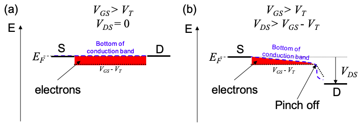
The threshold voltage, \(V_{T}\), is defined as the gate-source voltage required to turn the transistor ON, i.e. bring the bottom of the conduction band, \(E_{C}\), down to the source workfunction. From Equation (5.13.6) and requiring the \(E_{C}+U=\mu_{S}\) at threshold, we get
\[ V_{T} = (E_{C}-\mu_{S})/\eta^{0}q \nonumber \]
Above threshold the density of states and hence the quantum capacitance is constant. Thus, the quantum well FET is the rare case where we can model charging phenomena analytically. Above threshold we have
\[ U = -\eta q(V_{GS}-V_{T})-\eta^{0}qV_{T} \nonumber \]
where again we neglect the effect of \(V_{DS}\), and
\[ \eta=\frac{C_{G}}{C_{S}+C_{D}+C_{G}+C_{Q}} \nonumber \]
From the 2-d DOS in Equation (2.12.4), \(C_{Q}\) for a single mode quantum well is
\[ C_{Q} = \frac{1}{2}q^{2}\frac{mWL}{\pi \hbar^{2}} . \nonumber \]
where we have only considered half the usual density of states (the +k states). This is accurate in the saturation region because the drain cannot fill any states in the channel. The quantum capacitance increases in the linear region as the drain fills some –k states leading to errors in the calculation of the current in the linear regime.
Noting that \(V_{T} = E_{C}/\eta^{0}q\) we can rewrite Equation (5.13.9) above threshold as
Now, we can simplify Equation (5.13.5) to give us
\[ I=\frac{q W}{\pi^{2} \hbar^{2}} \int_{\mu_{s}-\eta q\left(V_{G s}-V_{T}\right)}^{\infty} \sqrt{2 m\left(E+\eta q\left(V_{G S}-V_{T}\right)\right)}\left(f\left(E, \mu_{S}\right)-f\left(E, \mu_{D}\right)\right) d E \nonumber \]
At T = 0K, we can solve Equation (5.13.13) in the linear regime (\(V_{DS}<\eta(V_{GS}-V_{T})\)):
\[ I = \frac{qW}{\pi^{2}\hbar^{2}} \int^{\mu_{S}}_{\mu_{S}-qV_{DS}} \sqrt{2m(E-E_{C} + \eta qV_{GS}))}dE \nonumber \]
\( \frac{qW}{\pi^{2}\hbar^{2}} \sqrt{\frac{8m}{9}} (\eta q)^{3/2} \left[ (V_{GS}-V_{T})^{3/2}-(V_{GS}-V_{T}-V_{DS}/\eta)^{3/2} \right] \)
and in the saturation regime \((V_{DS} > \eta (V_{GS}-V_{T}))\):
\[ \begin{aligned}
I &=\frac{q W}{\pi^{2} \hbar^{2}} \int_{\mu_{s}-\eta q\left(V_{G S}-V_{T}\right)}^{\mu_{S}} \sqrt{2 m\left(E+\eta q\left(V_{G S}-V_{T}\right)\right)} d E \\
&=\frac{q W}{\pi^{2} \hbar^{2}} \sqrt{\frac{8 m}{9}}(\eta q)^{3 / 2}\left(V_{G S}-V_{T}\right)^{3 / 2}
\end{aligned} \nonumber \]
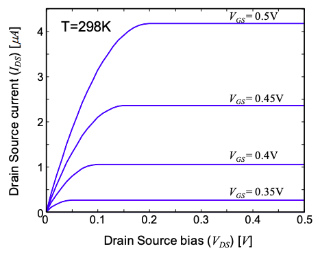
Note that the saturation current goes as \(\sim (V_{GS}-V_{T})^{3/2}\) compared to the ballistic nanowire transistor, which goes as \(\sim (V_{GS}-V_{T})\). As we shall see, the conventional FET has a saturation current dependence of \(\sim (V_{GS}-V_{T})^{2}\).
Conventional MOSFETs
Finally, we turn our attention to the backbone of digital electronics, the non-ballistic metal oxide semiconductor field effect transistor (MOSFET).
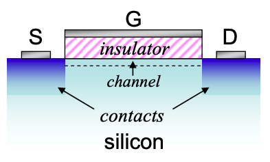
The channel material is a bulk semiconductor – typically silicon. Here, we will consider a so-called n-channel MOSFET, meaning that the channel current is carried by electrons at the bottom of the conduction band of the semiconductor.
Now, let's consider the various operating regimes of a conventional MOSFET.
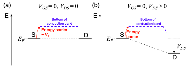
OFF: Subthreshold \(V_{GS} < V_{T}\)
Similar to the ballistic quantum wire FET, we can model channel current as injection over a barrier close to the source electrode.
Once again, let's define the threshold voltage as the potential difference between the source Fermi energy and the conduction band minimum.\(^{†}\)
As in the ballistic example, when \(V_{GS} < V_{T}\), only the tail of the Fermi distribution for electrons in the source overlaps with empty states in the conduction band. The current follows Equation (5.8.6).
\[ I = I_{0}\text{exp}\left[ \frac{qV_{GS}}{kT}\frac{C_{G}}{C_{ES}} \right] \nonumber \]
Subthreshold characteristics determine the gate voltage required to switch the FET ON and OFF. From Eq. (5.8.8) the subthreshold slope is ideally 60mV/decade, meaning that a 60mV change in gate potential corresponds to a decade change in channel current.
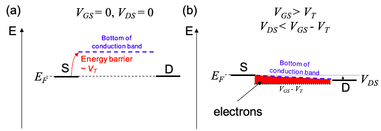
The linear regime: \(V_{GS} > V_{T},\ V_{DS} < V_{GS}-V_{T}\)
As we shall see, this is known as the linear regime because the current scales linearly with the drain source potential. Consider a thin slice of the channel with width W, and length \(\delta x\). For this analysis to hold, the length of this slice cannot be much shorter than the mean free path of the electron between scattering events. In a silicon transistor, we have shown that \(\delta x > 50 \text{nm}\) (see the analysis associated with Figure 4.14.3). Silicon transistors with channel lengths shorter than this should be analyzed in the ballistic regime.
Since the density of states above the conduction band is very large in a bulk semiconductor, a conventional MOSFET will enter the strong charging/metallic limit for \((V_{GS} – V) > V_{T}\), i.e. the number of charges, \(\delta N\), in the slice is
\[ q \delta N = \frac{C_{G}}{A}W\delta x(V_{GS}-V-V_{T}) \nonumber \]
where A = W.L is the surface area of the channel.
Now the current within the slice is given by
\[ I = \frac{q \delta N}{\tau} \nonumber \]
where \(\tau\) is the lifetime of carriers within the channel slice.
Since scattering is important, we employ the classical model of charge transport to relate the charge carrier lifetime to velocity, v, and the length of the slice, \(\delta x\).
\[ I = q \delta N\frac{v}{\delta x} \nonumber \]
Next we relate the charge carrier velocity to mobility
\[ I = q \delta N\frac{\mu F}{\delta x} \nonumber \]
Now, we must note that scattering causes the potential in the channel to vary with position. We define the channel potential V(x) as a function of position in the channel. Thus, expressing the source-drain electric field in terms of the channel potential we have
\[ I = q \frac{\mu}{\delta x}\delta N\frac{\delta V}{\delta x} \nonumber \]
Next, we substitute Equation (5.13.14) into Equation (5.13.15), yielding
\[ I = \mu \frac{C_{G}}{L}(V_{GS}-V-V_{T})\frac{\delta V}{\delta x} \nonumber \]
We solve this under the limit that \(\delta x \ll L\), by integrating both sides with respect to x. Since the current is uniform throughout the channel, we obtain:
\[ I.L = \int^{L}_{0} \mu \frac{C_{G}}{L}(V_{GS}-V-V_{T})\frac{dV}{dx} dx \nonumber \]
where L is the length of the channel. It is convenient to change the variable of integration on the righthand side to voltage. In the linear regime, the maximum channel potential is \(V_{DS}\), hence:
\[ I = \mu \frac{C_{G}}{L^{2}}\int^{V_{DS}}_{0} (V_{GS}-V-V_{T})dV \nonumber \]
The linear regime requires that the entire channel remains in the strong charging/metallic limit. This occurs if the gate to drain potential, \(V_{GD}\), also exceeds \(V_{T}\)
\[ V_{GD}>V_{T} \nonumber \]
or we can re-write this as
\[ V_{DS}<V_{GS}-V_{T} \nonumber \]
Under this constraint, Equation (5.13.21) yields
\[ I = \mu \frac{C_{G}}{L^{2}} \left( (V_{GS}-V_{T})V_{DS}-\frac{1}{2}V_{DS}^{2} \right) \nonumber \]
It is standard to express this in terms of a gate capacitance per unit channel area, \(C_{OX}\):
\[ I = \mu \frac{W}{L}C_{OX} \left( (V_{GS}-V_{T})V_{DS}-\frac{1}{2}V_{DS}^{2} \right) \nonumber \]
Saturation: \(V_{GS} > V_{T},\ V_{DS} > V_{GS}-V_{T}\)
If the gate to drain potential exceeds threshold then the channel region close to the drain enters the zero charging regime, characterized by a high electric field and low density of mobile charges. The channel is said to pinch off and the current saturates because it is no longer dependent on \(V_{DS}\). The strong charging/metallic region ends when the local channel potential \(V = V_{GS} - V_{T}\)
\[ I = \int^{V_{GS}-V_{T}}_{0}\mu \frac{W}{L}C_{OX}(V_{GS}-V-V_{T})dV \nonumber \]
which gives
\[ I = \mu \frac{W}{L}\frac{C_{OX}}{2}(V_{GS}-V_{T})^{2} \nonumber \]
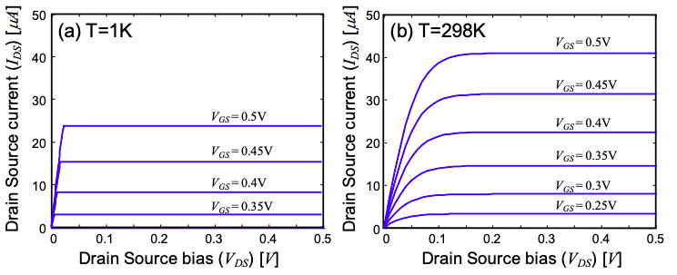
The IV characteristics of a non-ballistic MOSFET are shown in Figure 5.13.6.
\(^{†}\) Actually, this is an overestimate of the threshold voltage because the density of states at the conduction band is so large that the transistor will often turn on when the Fermi level gets within a few kT. It also ignores the effect of charge trapped at the interface between the channel and the insulator.