1.4: P-N Junction, Part I
- Page ID
- 88609

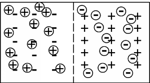
We are now ready to make an actual useful device! Let's take a piece of n-type material, and a piece of p-type material, and stick them together, as shown in Figure \(\PageIndex{2}\). This way we will be making a p-n junction, or diode, which will be our first real electric device other than a simple resistor.
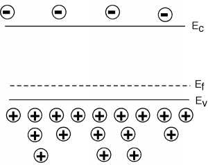
There are a couple of things wrong with Figure \(\PageIndex{2}\). First of all, one of the rules regarding the Fermi level is that when you have a system at equilibrium (that is, when it is at rest, and is not being influenced by external forces such as thermal gradients, electrical potentials etc.), the Fermi level must be the same everywhere. Secondly, we have a big bunch of holes on the right and a big bunch of electrons on the left, and so we would expect, that in the absence of some force to keep them this way, they will start to spread out until their distribution is more or less equal everywhere. Finally, we remember that a hole is just an absence of an electron, and since an electron in the conduction band can lower the system energy by falling down into one of the empty hole states, it seems likely that this will happen. This process is called recombination. The place where this is most likely to occur, of course, would be right at the junction between the n and p regions. This is shown in Figure \(\PageIndex{3}\).
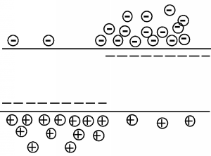
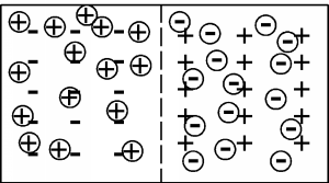
Now is might seem that this recombination effect might just go on and on, until there are no carriers left in the sample. This is not the case, however. In order to see what brings everything to a halt, we need yet another diagram. Figure \(\PageIndex{4}\) is more physical than what we have been looking at so far. It is a picture of the actual p-n junction, showing both the holes and the electrons. We also need to put in the donors and acceptors, however, if we want to see what goes on. The fixed (meaning they can't move around) charges of the donors and acceptors are represented by simple "+" and "-" signs. They are arranged in a nice lattice-like arrangement to remind us that they are stuck to the crystal lattice. (In reality however, even though they are stuck in the crystal lattice, there are so few of them compared to the silicon atoms that their distribution would be quite random.) For the mobile holes and electrons, we will stay with the little circles with charge signs in them. These are randomly distributed, to remind us that they are free to move about the crystal.
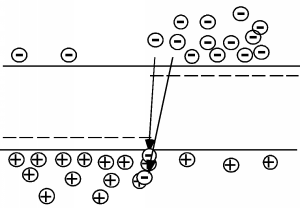
We will now have to allow some of the holes and electrons (again near the junction) to recombine. Remember, when an electron and a hole recombine, they both are annihilated and disappear. Note that this process conserves charge and (if we could calculate it) momentum as well. There is obviously some energy lost, but this will simply show up as vibrations, or heat, within the crystal lattice — or, in the case of an LED, as light emitted from the device. See, already we know enough about semiconductors to understand (somewhat) how an actual device works. Light coming from an LED is simply the energy which is released when an electron and hole recombine. We will take a look at this in more detail later. Let's allow some recombination to occur, as shown in Figure \(\PageIndex{5}\).