1.5: P-N Junction, Part II
- Page ID
- 88610

If you look closely at these pictures, you will notice something. As we remove more and more electrons and holes, we are starting to "uncover" the fixed charges associated with the donors and acceptors. We are making what is known as a depletion region, so named because it is depleted of mobile carriers (holes and electrons). The uncovered net charge in the depletion region is separated, with negative charge in the p-region, and positive charge in the n-region. What will such a charge separation give rise to? Why, an electric field! Of course! Which way will the field point? The electric field which arises from a separation of charges always goes from the positive charge, towards the negative charge. This is shown in Figure \(\PageIndex{1}\).
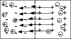
What effect will this field have on our device? It will have the tendency to push the holes back into the p-region and the electrons into the n-region. This is just what we need to counteract the recombination which has been going on, and hopefully bring it to a stop.
Now try to think through what effect this field could have on our energy band diagram. The band diagram is for electrons, so if an electron moves from the right hand side of the device (the n-region) towards the left hand side (the p-region), it will have to move through an electric field which is opposing its motion. This means it has do some work, or in other words, the potential energy for the electron must go up. We can show this on the band diagram by simply shifting the bands on the left hand side upward, to indicate that there is a shift in potential energy as electrons move from right to left across the junction.
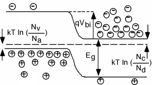
The shift of the bands, which is just the difference between the location of the Fermi level in the n-region and the Fermi level in the p-region, is called the built-in potential, \(V_{\mathrm{BI}}\). This built-in potential keeps the majority of holes in the p-region, and the electrons in the n-region. It provides a potential barrier, which prevents current flow across the junction. (On the band diagram we have to multiply the built-in potential \(V_{\mathrm{BI}}\) by the charge of an electron, \(q\), so that we can represent the shift in energy in terms of electron volts, the unit of potential energy used in band diagrams.)
How big is \(V_{bi}\)? This is not too hard to figure out. Let's look at Figure \(\PageIndex{2}\) a little more carefully. Remember, we know from Equation \(1.3.7\) that since \(n=N_{d}\) in the n-region and \(p=N_{a}\) in the p-region, we can relate the distance of the Fermi level from \(E_{c}\) and \(E_{f}\) by \[E_{c} - E_{f} = kT \ln \left( \frac{N_{c}}{N_{d}}\right) \nonumber \] and \[E_{f}-E_{v} = kT \ln \left(\frac{N_{v}}{N_{a}}\right) \nonumber \] Look at Figure \(\PageIndex{2}\) and see if you can agree that \[\begin{array}{l} qV_{\mathrm{BI}} &= \ E_{g} - \left(E_{c}-E_{f}\right) - \left(E_{f}-E_{v}\right) \\ &= \ E_{g}-kT \ln \left(\frac{N_{c}}{N_{d}}\right) - kT \ln \left(\frac{N_{c}}{N_{d}}\right) \\ &= \ E_{g} - kT \ln \left(\frac{N_{c} N_{v}}{N_{d} N_{a}}\right) \end{array} \nonumber \]
where the \(N_{d}\) and \(N_{a}\) are the doping densities in the n and p regions respectively. Remember that \(kT=1/40 \mathrm{~eV} = 0.025 \mathrm{~eV}\), \(E_{g} = 1.1 \mathrm{~eV}\), and \(N_{c}\) and \(N_{v}\) are both \(\approx \left(10^{19}\right)\). Thus, \[q V_{\mathrm{BI}} = 1.1 \mathrm{~eV} - 0.025 \mathrm{~eV} \cdot \ln \left(\frac{10^{38}}{N_{d} N_{a}}\right) \nonumber \]
Here the \(q\) in front of the \(V_{\mathrm{BI}}\) and the \(e\) in \(\mathrm{eV}\) are both the charge of 1 electron, and they cancel out, making \[V_{\mathrm{BI}} = \left(1.1 - 0.025 \ln \left(\frac{10^{38}}{N_{d} N_{a}}\right) \right) \mathrm{~volts} \nonumber \]
Suppose both \(N_{d}\) and \(N_{a}\) are both about \(10^{15}\) — not uncommon values. How big would the built-in potential be in this case?
It turns out that we can actually derive some specific details about the depletion region if we make only a couple of simplifying (and often justified) assumptions. In order to make the math easier, and also because many p-n junctions are built this way, we will consider what is known as a one-sided junction. Figure \(\PageIndex{3}\) is a picture of such a beast: In this diode, one side is much more heavily doped than the other. In this particular example, the p-side is heavily doped, and the n-side is relatively lightly doped. We can not show the true picture here, because typically, the more heavily doped side will be doped several orders of magnitude greater than the lightly doped side. Typical values might be \(N_{a}=10^{19}\) and \(N_{d}=10^{16}\). Regardless of how big the difference is, however, there must be exactly the same amount of "uncovered" charge on both side of the junction. Why? Because each time a hole and electron recombine to form the depletion region, they each leave behind either a donor or an acceptor. A careful count of the exposed charge in Figure \(\PageIndex{3}\) shows that I was careful enough to draw my figure accurately for you. We do not need to have a one-sided diode to do the analysis that will follow, but the equations are easier to solve if we do.
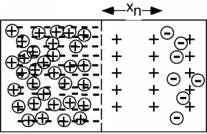
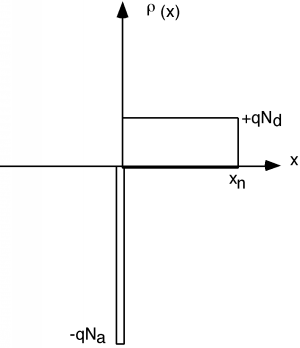
In order to proceed from here, the first thing we do is make a plot of the charge density \(\rho (x)\) as we move through the junction. Naturally, in the bulk, since the holes and the acceptors (in the p-side), or the electrons and the donors (in the n-side) just equal one another, the net charge density is zero. In the depletion region, the charge density is \(\left(-q\right) N_{a}\) on the p-side and \((q) N_{d}\) on the donor side. (All the mobile carriers are gone, and we are left with just the charged acceptors or donors.) We will make the assumption that on the n-side, the depletion extends a distance \(-x_{n}\) from the junction. On the p-side, the acceptor charge density is so large that we will treat it is a \(\delta\)-function, with essentially no width. The areas of the two boxes must be the same (equal amount of positive and negative charge) and hence, the tall thin box actually has a width of \(\frac{N_{d}}{N_{a}} x_{n}\) which, since \(N_{a}\) is several orders of magnitude greater than \(N_{d}\), means that the tall box has a very, very small width compared to the lower, wider one, which is \(q N_{d}\) tall, and has a width of \(x_{n}\).