
1.7: Depletion Width
- Page ID
- 88615

We can now go back to the charge density as a function of position graph and easily find the electric field in the depletion region as a function of position. If we integrate Gauss's Law, we get for the electric field: \[\mathbf{E} (x) = \frac{1}{\varepsilon} \int \rho(x) \ dx \nonumber \]
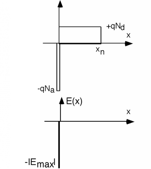
We could write down an expression for \(\rho(x)\) and then formally integrate it to get \(\mathbf{E} (x)\) but we can also just do it graphically, which is a lot easier, and gives us a much more intuitive feeling for what is going on. Let's start doing our integral at \(x \rightarrow \infty\). Whenever we perform an integral such as Equation \(\PageIndex{1}\), we've got to remember to add a constant to our answer. Since we cannot have an electric field which extends to infinity (either plus or minus), however, we can safely assume \(\mathbf{E} (- \infty)\) and remains at that value until we get to the edge of the depletion region at (essentially) \(x=0\). Since the charge density is zero all the way up to the edge of depletion region, Gauss tells us that the electric field can not change here either. When we get to \(x=0\) we encounter the large negative delta-function of negative charge at the edge of the depletion region. If you can remember back to your calculus, when you integrate a delta function, you get a step. Since the charge in the p-side delta function is negative, when we integrate it, we get a negative step. Since we don't know (yet) how big the step will be, let's just call it \(- \left| E_{\max} \right|\).
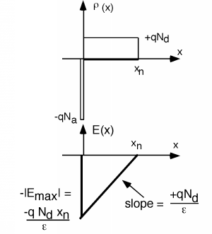
In the n-side of the depletion region, \[\begin{array}{l} \rho(x) &= (q) N_{d} \\ &= \varepsilon \dfrac{\delta \mathbf{E}}{\delta x} \end{array} \nonumber \]
and so we plot \(\mathbf{E}(x)\) with a (positive) slope of \(\frac{q N_{d}}{\varepsilon}\) starting at \(E(x) = - E_{\max}\) at \(x=0\). This line continues with this positive slope until it reaches a value of \(0\) at \(x_{n}\). We know that \(E(x)\) must equal \(0\) at \(x = x_{n}\) because there is no further charge outside of the depletion region and \(E\) must be \(0\) outside this region.
We are now done doing the integral. We would know everything about this problem, if we just knew what \(x_{n}\) was. Note that since we know the slope of the triangle now, we can find \(-E_{\max}\) in terms of the slope and \(x_{n}\). We can derive an expression for \(x_{n}\), if we remember that the integral of the electric field over a distance is the potential drop across that distance. What is the potential drop in going from the p-side to the n-side of the diode?
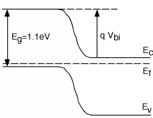
As a reminder, Figure \(\PageIndex{3}\) shows the junction band diagram again. The potential drop must just be \(V_{\mathrm{bi}}\), the "built-in" potential of the junction. Obviously \(V_{\mathrm{bi}}\) can not be greater than \(1.1 \mathrm{~V}\), the band-gap potential. On the other hand, by looking at Figure \(\PageIndex{3}\), and remembering that the band gap in silicon is \(1.1 \mathrm{~eV}\), it will not be some value like 0.2 or 0.4 volts either. Let's make life easy for ourselves, and say \(V_{\mathrm{bi}} = 1 \mathrm{~Volt}\). This will not be too far off, and as you will see shortly, the answer is not very sensitive to the exact value of \(V_{\mathrm{bi}}\) anyway.
The integral of \(\mathbf{E}_{x}\) is now just the area of the triangle in Figure \(\PageIndex{2}\). Getting the area is easy: \[\begin{array}{l} \text{area} &= \frac{1}{2} \text{ base} \times \text{height} \\ &= \frac{1}{2} \ x_{n} \frac{q N_{d} x_{n}}{\varepsilon} \\ &= \frac{q N_{d} x_{n}^2}{2 \varepsilon} \\ &= V_{\mathrm{bi}} \end{array} \nonumber \]
We can simply turn Equation \(\PageIndex{3}\) around and solve for \(x_{n}\). \[x_{n} = \sqrt{ \frac{2 \varepsilon V_{\mathrm{bi}}}{q N_{d}} } \nonumber \]
As we said, for silicon, \(\varepsilon_{\mathrm{Si}} = 1.1 \times 10^{-12}\). Let's let \(N_{d} = 10^{16} \mathrm{~cm}^{-3}\) donors. As we already know from before, \(q = 1.6 \times 10^{-19} \mathrm{~Coulombs}\). This makes \(x_{n} = 3.7 \times 10^{-5} \mathrm{~cm}\) or \(0.37 \ \mu \mathrm{m}\) long. Not a very wide depletion region! How big is \(\left| E_{\max} \right|\)? Plugging in \[E_{\max} = \frac{q N_{d} x_{n}}{\varepsilon} \nonumber \]
we find that \(\left| E_{\max} \right| = 53,000 \ \frac{\mathrm{V}}{\mathrm{cm}}\)! Why such a big electric field? Well, we've got to shift the potential by about a volt, and we do not have much distance to do it in (less than a micron), and so there must be, by default, a fairly large field in the depletion region. Remember, potential is electric field times distance.
Enough p-n junction electrostatics. The point of this exercise was twofold; so you would know something about the details of what is really going on in a p-n junction to show you that with just some very simple electrostatics and a little thinking, it is not so hard to figure these things out!